Method for manufacturing semiconductor device

Active Publication Date: 2005-11-17
DONGBU ELECTRONICS CO LTD +1
View PDF2 Cites 11 Cited by
  • Summary
  • Abstract
  • Description
  • Claims
  • Application Information

AI Technical Summary

Benefits of technology

[0011] The present invention has been made in an effort to provide a method for forming an OSG that is novel and provid

Problems solved by technology

Nevertheless, a drawback of copper is that, unlike with tungsten and aluminum, it is difficult to form lines in semiconductor devices by reactive ion etching.
In this case, a source m

Method used


Image

  • Method for manufacturing semiconductor device
  • Method for manufacturing semiconductor device
  • Method for manufacturing semiconductor device

Examples


Embodiment Construction

[0019] An embodiment of the present invention will hereinafter be described in detail with reference to the accompanying drawings.

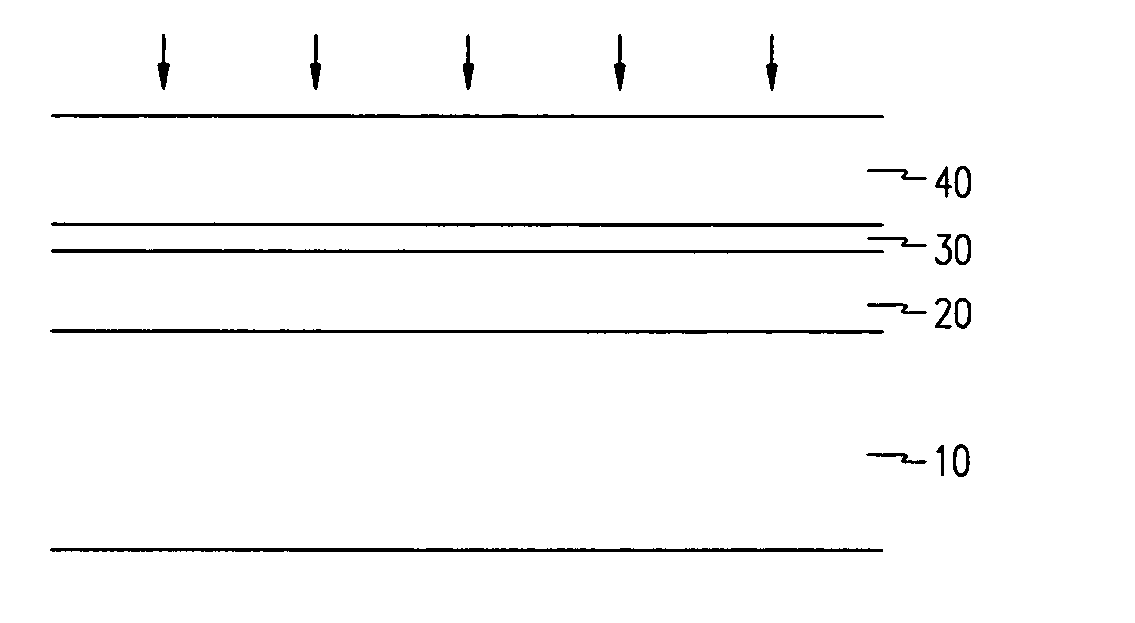
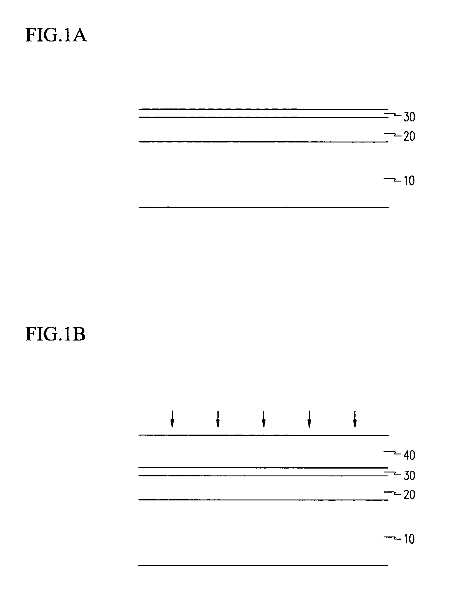
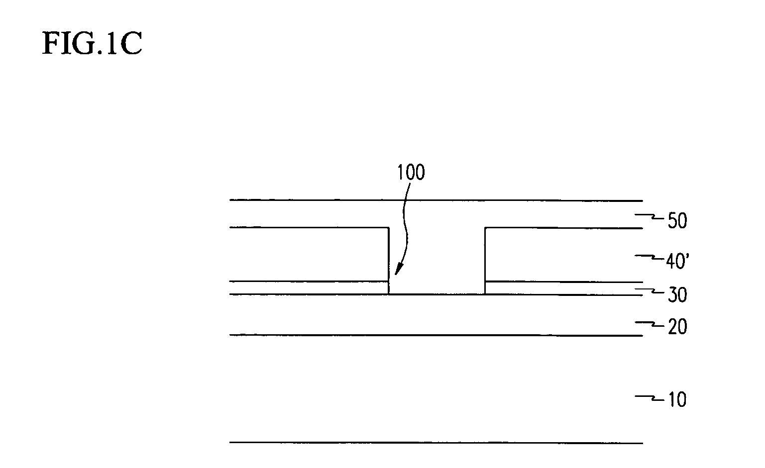
[0020]FIG. 1A to FIG. 1C are sectional views illustrating a method for manufacturing a semiconductor device according to an embodiment of the present invention.

[0021] Firstly, as shown in FIG. 1A, a lower wire layer 20 is formed on a structure 10 comprising a semiconductor substrate.

[0022] In this case, the structure 10 may include a device such as a transistor, comprising a gate oxide layer and a gate electrode formed on the semiconductor substrate, and source and drain regions formed in the substrate. In addition, it may also include a lower insulating layer formed above the individual device.

[0023] The lower wire layer 20 may comprise a metal material such as copper, aluminum, or an aluminum alloy. Although not shown in FIG. 1A, when the lower wire layer 20 comprises or consists essentially of aluminum or an aluminum alloy, it may be patterned to a...


PUM


Abstract

High quality dielectric layers may be achieved without introducing excessive impurities when a semiconductor device is manufactured by a method that includes forming a lower wire layer on a structure above a semiconductor substrate, forming a silicon rich oxide layer having a refractive index of 0.45-1.55 on the lower wire layer and the structure, implanting carbon and oxygen (e.g., CO2) into the silicon rich oxide (SRO) layer, and forming an organosilicate glass layer by heat-treating the implanted SRO layer.

Description

CROSS-REFERENCE TO RELATED APPLICATION [0001] This application claims priority to and the benefit of Korean Patent Application 10-2004-0032924 filed in the Korean Intellectual Property Office on May 11, 2004, the entire content of which is incorporated herein by reference. BACKGROUND OF THE INVENTION [0002] (a) Field of the Invention [0003] The present invention relates to a method for manufacturing a semiconductor device. More particularly, the present invention relates to a method for forming an organosilicate glass (OSG) that may be used as an interlayer insulating layer in a device that contains copper lines. [0004] (b) Description of the Related Art [0005] Tungsten (W), aluminum (Al), and / or an aluminum alloy are typically used as the metal to form a metal line in a semiconductor device. However, much research is being undertaken on ways to use copper (Cu) in place of tungsten and aluminum for the metal wiring in semiconductor devices because of the relatively low resistivity o...

Claims


Application Information

Patent Timeline
IPC IPC(8): H01L21/3115H01L21/31H01L21/4763H01L21/768
CPCH01L21/76825H01L21/76801H01L21/31
Inventor LEE, JAE-SUK
Owner DONGBU ELECTRONICS CO LTD
Why Eureka
Try Eureka