
High-voltage ceramic capacitor

a high-voltage ceramic and capacitor technology, applied in the direction of fixing capacitor details, manufacturing tools, soldering apparatus, etc., can solve the problems of pb-less solder being very hard and not having enough extensibility, falling of the terminal, cracking or fracture of ceramic porcelain,

Active Publication Date: 2005-11-24
TDK CORPARATION
View PDF4 Cites 3 Cited by
  • Summary
  • Abstract
  • Description
  • Claims
  • Application Information

AI Technical Summary

Benefits of technology

[0008] It is an object of the present invention to provide a high-voltage ceramic capacitor in which a fall of the metal terminal and occurrence of a crack or a fracture in the ceramic porcelain are prevented.
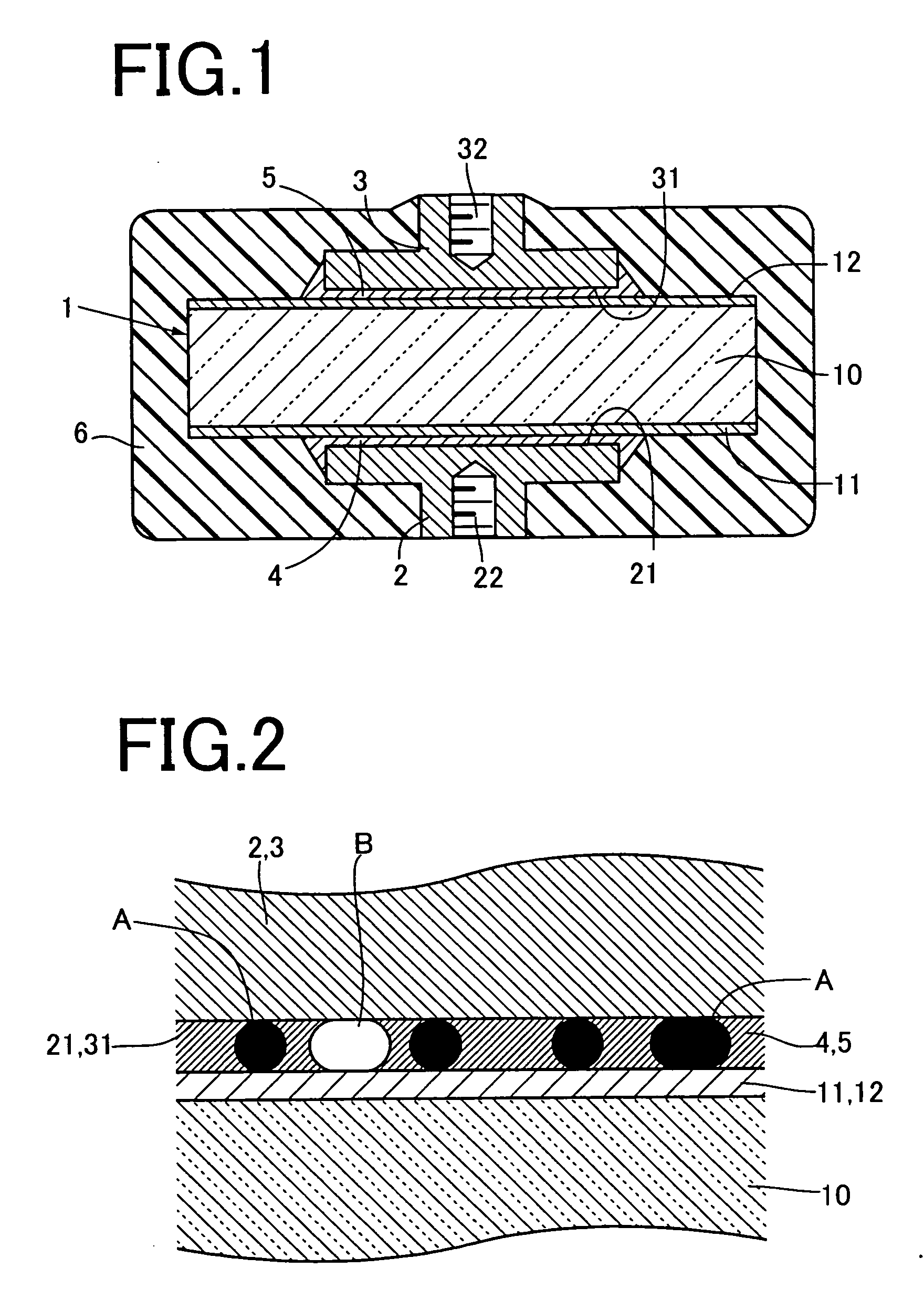
[0012] Thus, in the present invention, the solder constituting the solder joint portion contains inorganic particles having a melting point higher than a solder melting point. If the above-described inorganic particles are contained in the solder, the joining force is dispersed when shifting from a molten phase area to a solid phase area at the time of soldering, and hollow portions are partially generated. As a result, a stress generated due to a difference in linear expansion coefficient between the metal terminal and the ceramic porcelain can be alleviated, thereby solving the problem of a fall of the metal terminal or occurrence of a crack or a fracture in the ceramic porcelain.
[0013] As described above, the present invention provides a high-voltage ceramic capacitor in which a fall of the metal terminal or occurrence of a crack or a fracture in the ceramic porcelain are prevented.

Problems solved by technology

A problem lies in that the Pb-less solder is very hard and does not have enough extensibility as compared with lead solder.
Therefore, there has been a problem that a difference in thermal expansion coefficient between respective members cannot be absorbed or alleviated in or after soldering when the Pb-less solder is used, thereby resulting in a fall of the terminal or occurrence of a crack or a fracture of the ceramic porcelain.

Method used


Image

  • High-voltage ceramic capacitor
  • High-voltage ceramic capacitor
  • High-voltage ceramic capacitor

Examples


Embodiment Construction

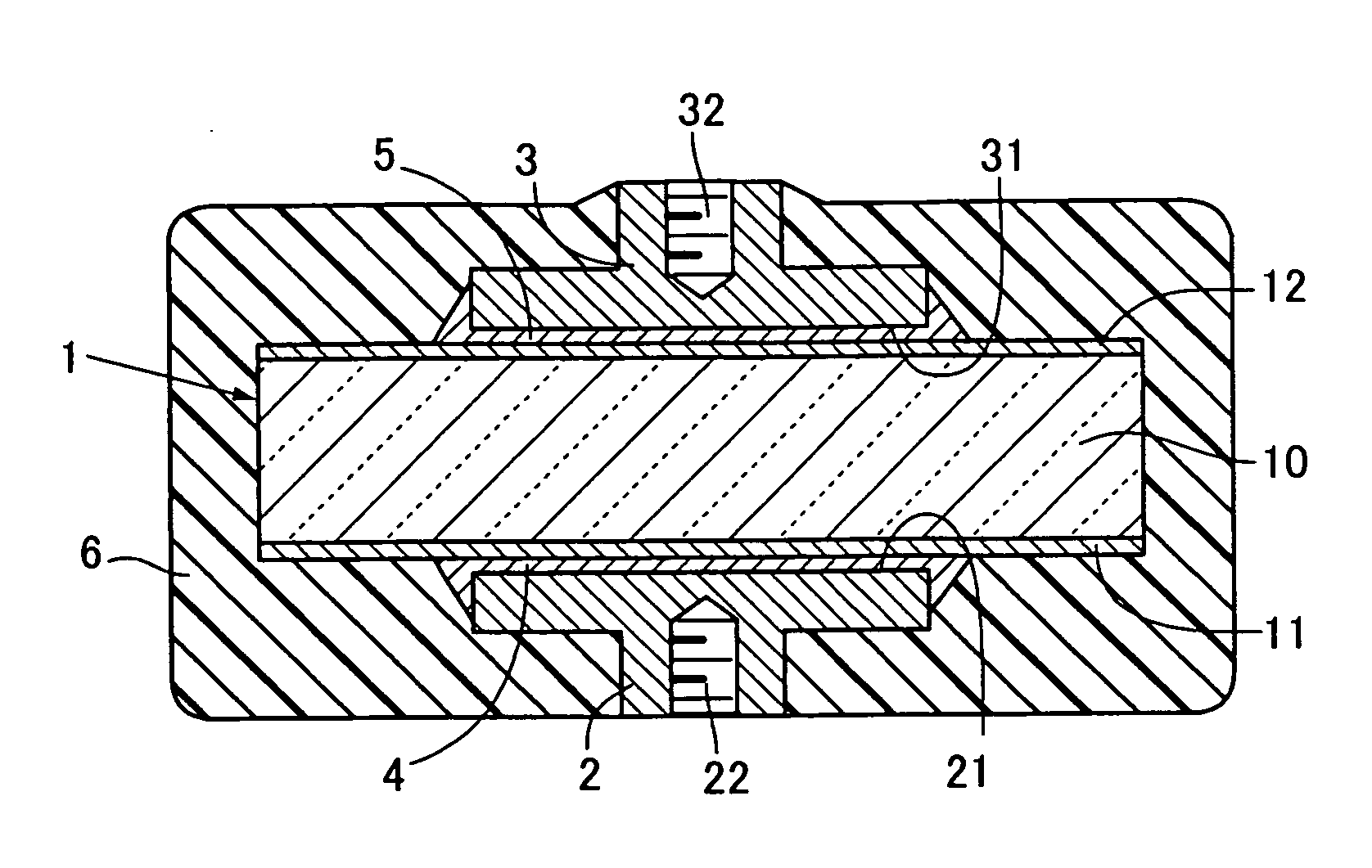
[0020]FIG. 1 is a front cross-sectional view showing an embodiment of a high-voltage ceramic capacitor according to the present invention, and FIG. 2 is a partially enlarged cross-sectional schematically showing the high-voltage ceramic capacitor depicted in FIG. 1. The illustrated high-voltage ceramic capacitor comprises a capacitor element 1, metal terminals 2 and 3, and solder joint portions 4 and 5. The entire high-voltage ceramic capacitor is covered with a well-known insulating resin 6 such as epoxy resin.

[0021] The capacitor element 1 has electrodes 11 and 12 on opposing surfaces of the ceramic porcelain 10. The ceramic element 1 is formed of a ceramic dielectric material such as BaTiO3 or SrTiO3. The electrodes 11 and 12 contain Ag, Cu, Ni / Sn or the like as a main component and are secured to both main surfaces of the ceramic element 1 by means such as baking.

[0022] The metal terminal 2 (or 3) has one end surface 21 (or 31) facing one surface of the electrode 11 (or 12). T...


PUM

PropertyMeasurementUnit
particle diameteraaaaaaaaaa
voltageaaaaaaaaaa
voltageaaaaaaaaaa

Abstract

A high-voltage ceramic capacitor which includes a capacitor element, at least one metal terminal, and at least one solder joint portion. The capacitor element has electrodes on opposing surfaces of a ceramic porcelain. The metal terminal has one end surface facing one surface of the electrode. The solder joint portion is interposed between one end surface of the metal terminal and one surface of the electrode, and solders both surfaces. The solder constituting the solder joint portion does not contain lead but inorganic particles having a melting point higher than a solder melting point.

Description

TECHNICAL FIELD [0001] The present invention relates to a high-voltage ceramic capacitor for an extra high voltage, which is used for, e.g., power signal separation, voltage division or a laser oscillation power supply. BACKGROUND OF THE INVENTION [0002] This type of high-voltage ceramic capacitor has a ceramic porcelain, electrodes (Ag, Cu, Ni / Sn or the like) provided on main surfaces of the ceramic porcelain, a metal terminal joined to each of the electrodes, and a resin coating closely provided on the dielectric ceramic and the electrodes over all. [0003] In the high-voltage ceramic capacitor, the metal terminal is generally soldered to the electrode by high-temperature processing. As solder used for the soldering, solder containing metallic lead (lead solder) has been conventionally employed. Since the lead solder is very soft and superior in elasticity, this material can absorb a difference in linear expansion coefficient between the ceramic and the metal terminal and prevent a...

Claims


Application Information

Patent Timeline
Patent Type & Authority Applications(United States)
IPC IPC(8): H01G4/12B23K35/26H01G4/008H01G4/06H01G4/228
CPCH01G4/228B23K35/26H01G4/1272
Inventor MIURA, IWAOSATO, TSUKASA
Owner TDK CORPARATION
Learn More