Radio wave reception device and radio wave clock
- Summary
- Abstract
- Description
- Claims
- Application Information
AI Technical Summary
Benefits of technology
Problems solved by technology
Method used
Image

Examples
first embodiment
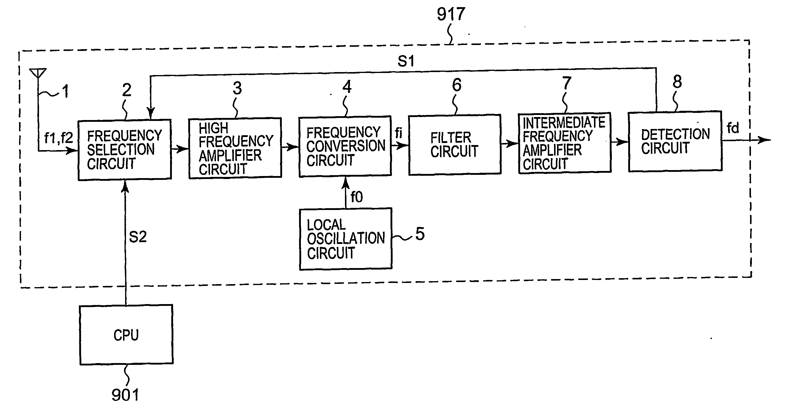
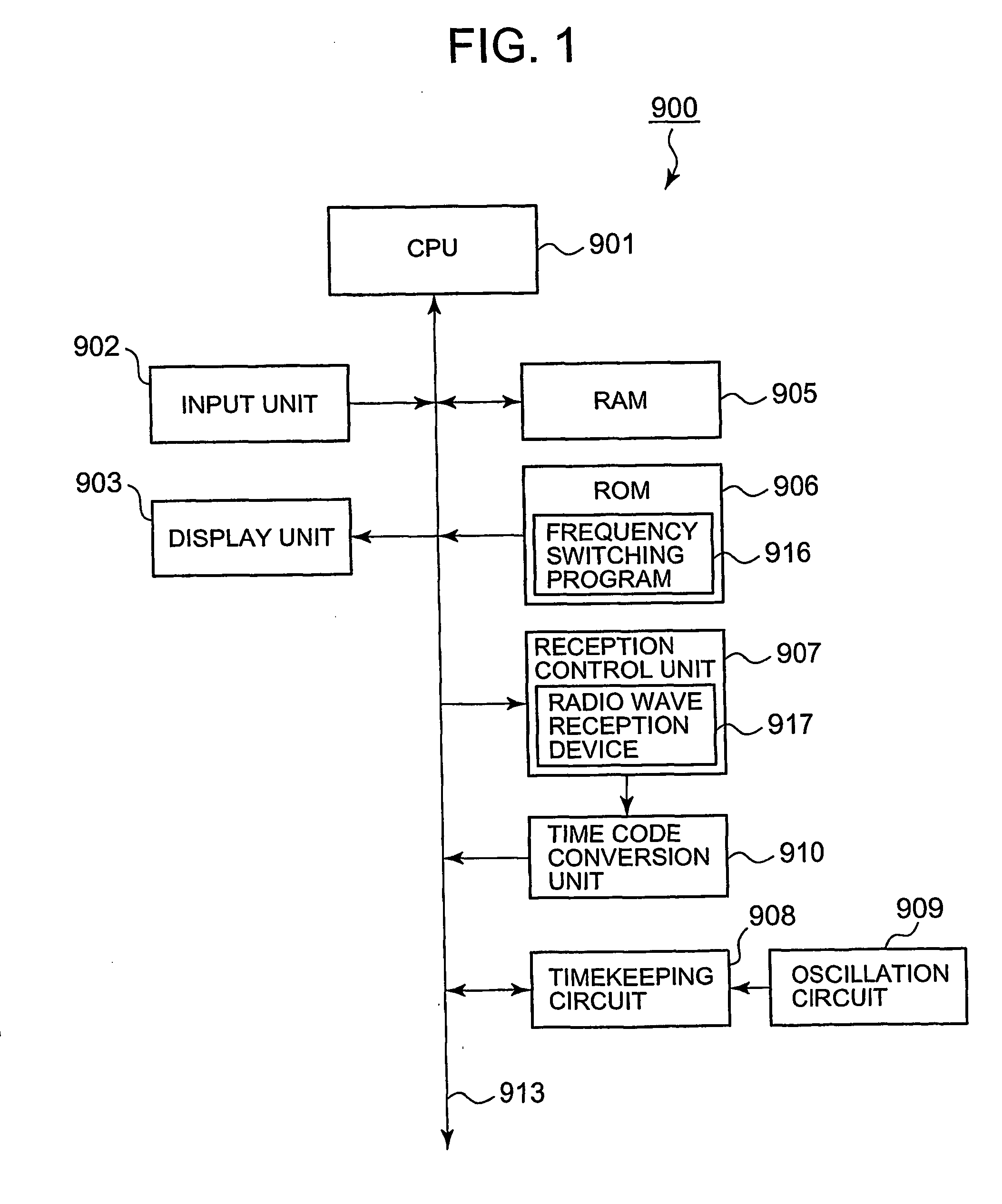
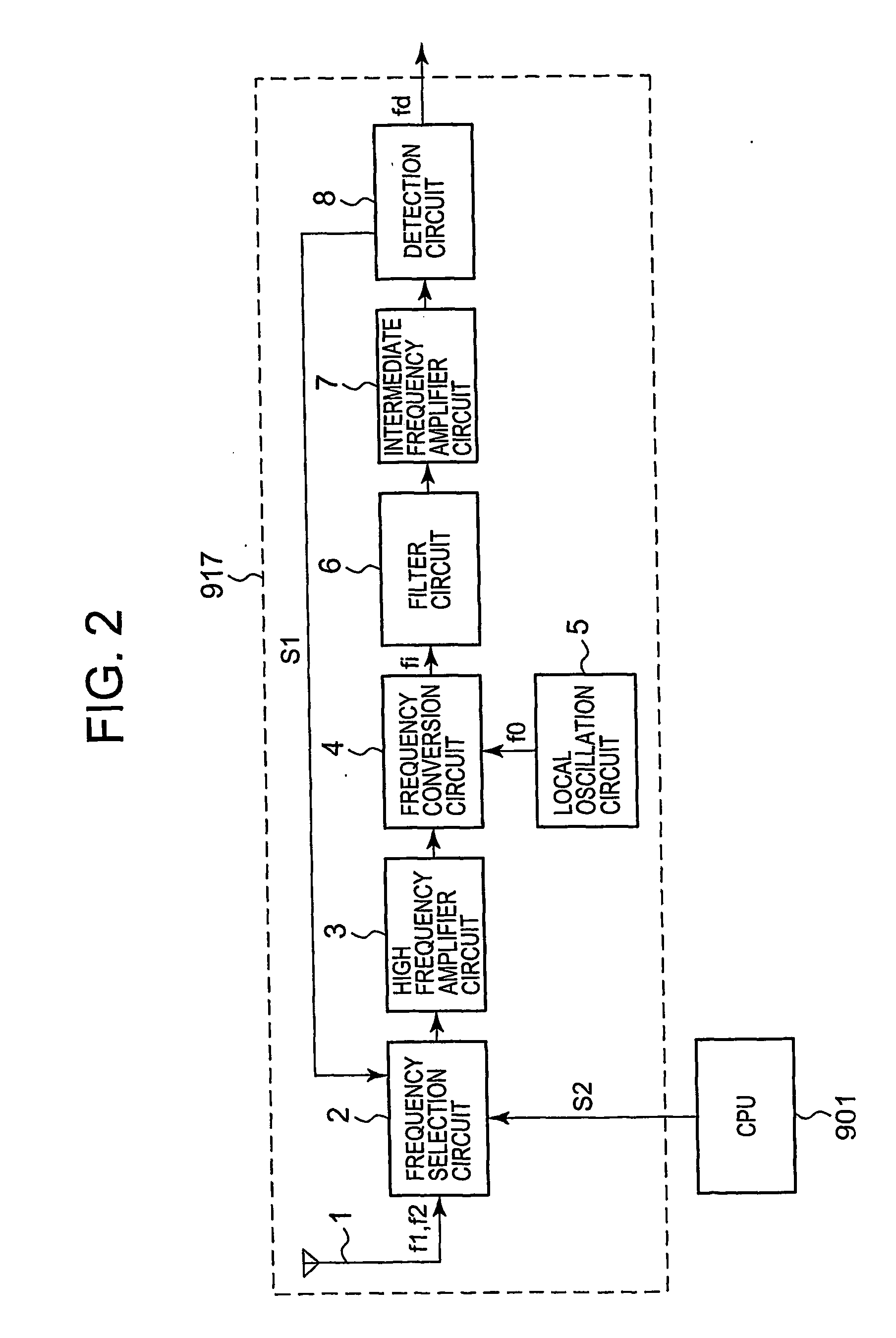
[0021]FIG. 1 is a diagram showing a circuit structure of a radio wave clock 900. The radio wave clock 900 comprises a CPU (Central Processing Unit) 901, an input unit 902, a display unit 903, a RAM (Random Access Memory) 905, a ROM (Read Only Memory) 906, a reception control unit 907, a timekeeping circuit 908, and a time code conversion unit 910. The respective units are connected by a bus 913. Further, an oscillation circuit 909 is connected to the timekeeping circuit 908.
[0022] The CPU 901 reads out various programs stored in the ROM 906 at a predetermined timing or in accordance with an operation signal and the like input from the input unit 902, and expands the read-out programs in the RAM 905 in order to give instructions or transfer data to each functional unit based on the programs. Particularly, the CPU 901 controls the reception control unit 907 at every predetermined interval to perform an operation for receiving a standard radio wave. Then, the CPU 901 corrects data rep...
second embodiment
[0053] Next, a second embodiment of the present invention will be explained. The structure of the radio wave clock according to the second embodiment is the same as that of the radio wave clock 900 shown in FIG. 1 except that a radio wave reception device 920 shown in FIG. 4 is prepared instead of the radio wave reception device 917. Accordingly, the same structural components will be denoted by the same reference numerals, and the explanation of such structural components will be omitted.
[0054]FIG. 4 is a block diagram showing the circuit structure of the radio wave reception device 920 according to the present embodiment. A synchronous detection circuit 10 detects a base band signal from a signal input from the intermediate frequency amplifier circuit 7 using a signal having the same frequency as a carrier wave, and outputs a signal having a frequency of fd to the time code conversion unit 910. The synchronous detection circuit 10 comprises an oscillation circuit 110 which oscill...
third embodiment
[0066] In the second embodiment, a signal having the local oscillation frequency f0 is generated by using the oscillation circuit 110 of the synchronous detection circuit 10. In the present embodiment, a radio wave reception device 930 that uses a signal output from the local oscillation circuit 5 for radio wave detection by the synchronous detection circuit 10, will be explained. The structure of a radio wave clock according to the third embodiment is the same as that of the radio wave clock 900 shown in FIG. 1, except that a radio wave reception device 930 shown in FIG. 5 is prepared instead of the radio wave reception device 917. Accordingly, the same structural components will be denoted by the same reference numerals, and explanation of such structural components will be omitted.
[0067]FIG. 5 is a block diagram showing the circuit structure of the radio wave reception device 930 according to the present embodiment. A synchronous detection unit 40 comprises a local oscillation c...
PUM
 Abstract
Description
Claims
Application Information
 - R&D Engineer
- R&D Manager
- IP Professional
- Industry Leading Data Capabilities
- Powerful AI technology
- Patent DNA Extraction
Browse by: Latest US Patents, China's latest patents, Technical Efficacy Thesaurus, Application Domain, Technology Topic.
© 2024 PatSnap. All rights reserved.Legal|Privacy policy|Modern Slavery Act Transparency Statement|Sitemap