Film formation source, vacuum film formation apparatus, organic EL panel and method of manufacturing the same

a film formation source and vacuum film technology, applied in vacuum evaporation coating, film formation source, organic el panel and manufacturing field, can solve the problems of increasing the size of the film formation apparatus, low pattern formation precision, and no suitable treatment method of substrate, etc., to achieve acceptable film formation precision, uniform film thickness, and uniform luminescence.

Inactive Publication Date: 2005-12-01
TOHOKU PIONEER CORP
View PDF8 Cites 92 Cited by
  • Summary
  • Abstract
  • Description
  • Claims
  • Application Information

AI Technical Summary

Benefits of technology

[0011] The present invention is to solve the above-discussed problem and it is an object of the invention to provide an improved vacuum film formation apparatus, organic EL panel and method of manufacturing the same, so that when performing film formation on a large size substrate, it is possible to ensure an acceptable film formation precision as well as a uniform film thickness, and that when forming organic EL devices on a large size substrate, it is possible to ensure a uniform luminescence as well as an acceptable color balance. Another object of the present invention is to increase the utilization efficiency of film formation material, thereby reducing the manufacturing cost.

Problems solved by technology

However, none of these methods is suitable for treating a substrate having a relatively large area.
This is because a large size substrate makes it necessary to enlarge a film formation area by enlarging the scale of a film formation source or increasing a distance between the substrate and the film formation source, hence resulting in an increase in the size of the film formation apparatus.
Moreover, if the substrate and a mask are brought close to each other in order to inhibit material consumption, film formation materials entering shielding portions of the mask are likely to cause a film formation defect, resulting in a low pattern formation precision and thus causing an un-uniform distribution of film thickness.
However, in a process of manufacturing such organic EL device, if the scale of the film formation source is increased in order to treat a large size substrate, a further problem will occur which shows that if an organic compound material exhibits a low thermal conductivity, it is difficult to ensure a uniform vapor deposition flow, making it impossible to realize a uniform film formation and thus reducing the function of the organic layer.
However, in the prior art disclosed in Japanese Unexamined Patent Application Publication No. 2001-247959, since the respective vapor deposition cells are arranged to be separated from one another at a predetermined pitch p, and since the respective vapor deposition cells are rendered responsible for forming film formation area in accordance with a predetermined film formation distribution perpendicular to the movement of vapor deposition source, film formation areas of vapor deposition cells mutually adjacent with each other in accordance with the pitch will be overlapped with one another, causing a problem that irregularities will occur and are distributed in thin film M corresponding to the pitch p.
Although the problem discussed above can be avoided by narrowing the pitch p as small as possible, the miniaturization of the pitch p (the width of which depends upon the width of vapor deposition cells) requires arranging many extremely small vapor deposition cells, resulting in a complicated management of the temperature of the respective vapor deposition cells.
Besides, there is a limitation in miniaturizing vapor deposition cells, and if the vapor deposition cells are miniaturized, it will be necessary to frequently supplement the film formation material, resulting in a low operation efficiency in film formation.
In addition, if the thickness of deposited film is not uniform, especially when forming an organic layer for organic EL device, the thickness of the formed organic layer in one luminescent area will be different from that of another, hence rendering it impossible to ensure a uniform luminescence or an acceptable color balance.
However, since the film formation flow emitted from the film formation source has a film formation distribution also in a direction perpendicular to the longitudinal direction (i.e., the longitudinal direction of the rectangle vapor deposition window) containing the film formation source, a considerable amount of the film formation material will be blocked by the shielding plate and thus will not be utilized in an actual film formation, resulting in a low efficiency in utilizing film formation material.
In particular, since an organic compound material for use in forming an organic layer in organic El device is usually expensive, there will be a problem that the manufacturing cost is high.

Method used


Image

  • Film formation source, vacuum film formation apparatus, organic EL panel and method of manufacturing the same
  • Film formation source, vacuum film formation apparatus, organic EL panel and method of manufacturing the same
  • Film formation source, vacuum film formation apparatus, organic EL panel and method of manufacturing the same

Examples


Embodiment Construction

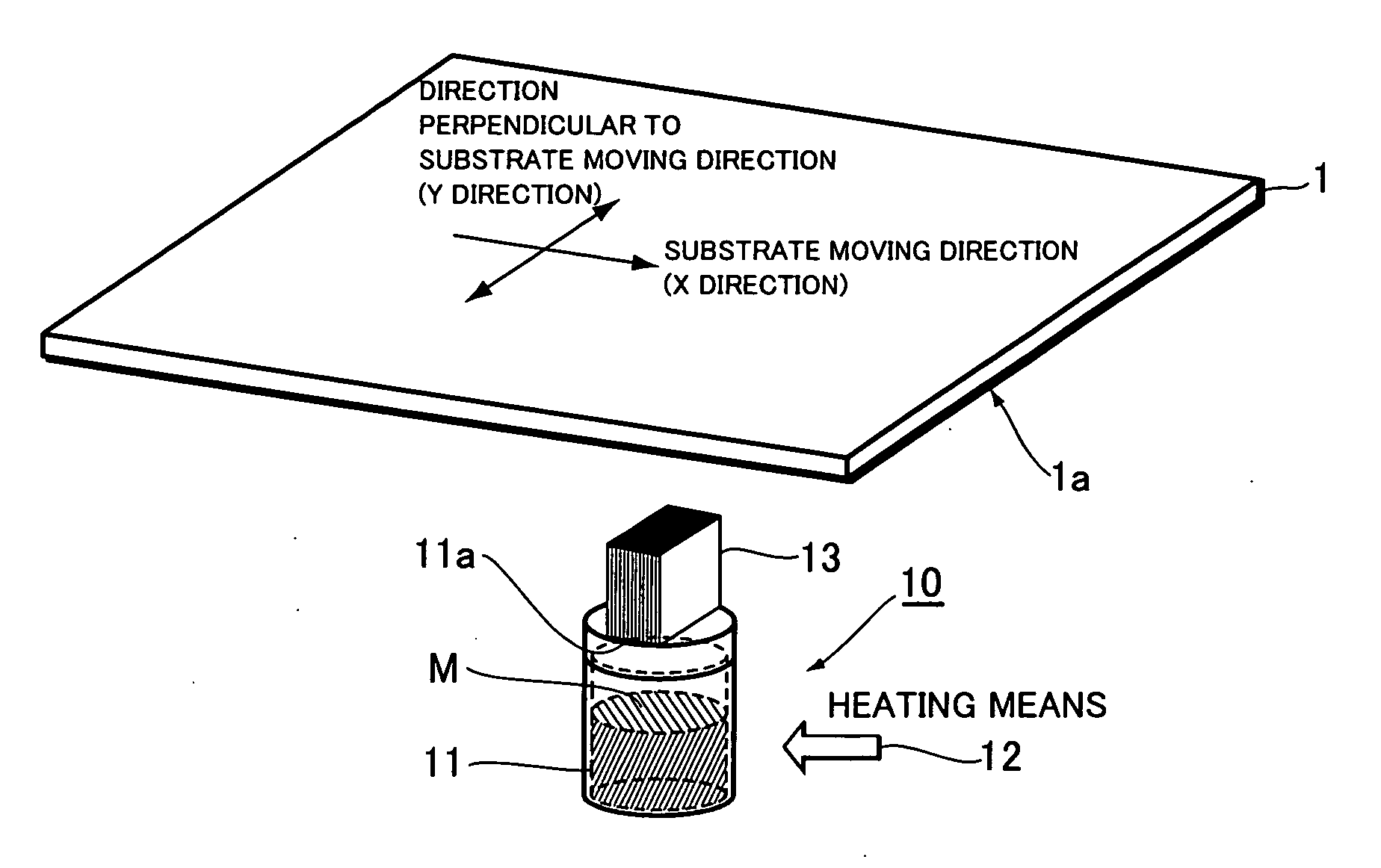
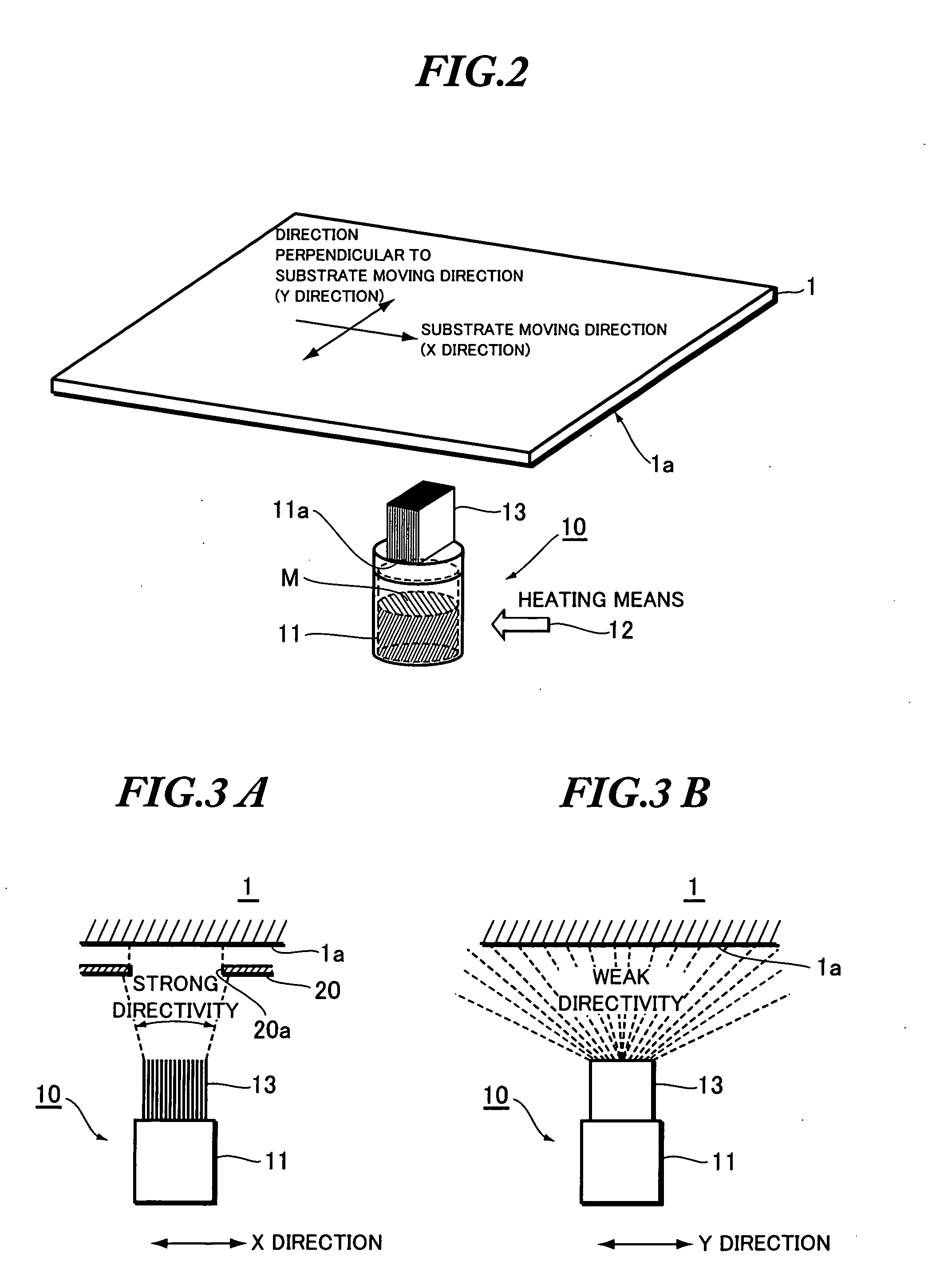
[0024] A preferred embodiment of the present invention will be described below with reference to the accompanying drawings. FIG. 2 and FIG. 3 are explanatory views showing a film formation source according to one embodiment of the present invention. As shown, a film formation source 10 comprises a material accommodating unit 11 for accommodating a film formation material M, heating means 12 for heating the film formation material M contained in the material accommodating unit 11, a film formation flow control unit 13 provided at an emission outlet 11a of the material accommodating unit 11 for controlling the direction of a film formation flow. In this way, a film formation flow formed by heating and thus sublimating or evaporating the film formation material M is caused to irradiate a film formation surface 1a of a substrate 1 being moved in X direction, thereby forming a thin film layer on the film formation surface 1a.

[0025] Here, the film formation flow control unit 13 operates ...


PUM

PropertyMeasurementUnit
luminescentaaaaaaaaaa
organicaaaaaaaaaa
areaaaaaaaaaaa

Abstract

A film formation source of a vacuum film formation apparatus for forming thin film on the film formation surface of a substrate comprises: a material accommodating unit containing a film formation material; heating means for heating the film formation material contained within the material accommodating unit; a film formation flow control unit provided at an emission outlet of the material accommodating unit for controlling the direction of the film formation flow. The film formation flow control unit provides a strong directivity to the film formation flow with respect to the moving direction of the film formation surface relative to the film formation source.

Description

BACKGROUND OF THE INVENTION [0001] The present invention relates to film formation source, vacuum film formation apparatus, organic EL panel and method of manufacturing the same. [0002] The present application claims priority from Japanese Application No. 2004-163413, the disclosure of which is incorporated herein by reference. [0003] A film formation method such as vapor deposition, sputtering, and molecular beam epitaxy and the like usually employs a single one fixed film formation source. However, none of these methods is suitable for treating a substrate having a relatively large area. This is because a large size substrate makes it necessary to enlarge a film formation area by enlarging the scale of a film formation source or increasing a distance between the substrate and the film formation source, hence resulting in an increase in the size of the film formation apparatus. Moreover, if the substrate and a mask are brought close to each other in order to inhibit material consum...

Claims


Application Information

Patent Timeline
Patent Type & Authority Applications(United States)
IPC IPC(8): C23C14/12H05B33/10C23C14/24C23C16/00H01L51/00H01L51/50H01L51/56H05B33/14
CPCC23C14/12C23C14/243Y10T428/10H01L51/0011H01L51/56H01L51/001C09K2323/00H10K71/164H10K71/166H10K71/00H05B33/10C23C14/24
Inventor MASUDA, DAISUKEABIKO, HIROSIUMETSU, SHIGEHIRO
Owner TOHOKU PIONEER CORP
Why Eureka
Try Eureka