Heterojunction field effect semiconductor device
- Summary
- Abstract
- Description
- Claims
- Application Information
AI Technical Summary
Benefits of technology
Problems solved by technology
Method used
Image
Examples
first embodiment
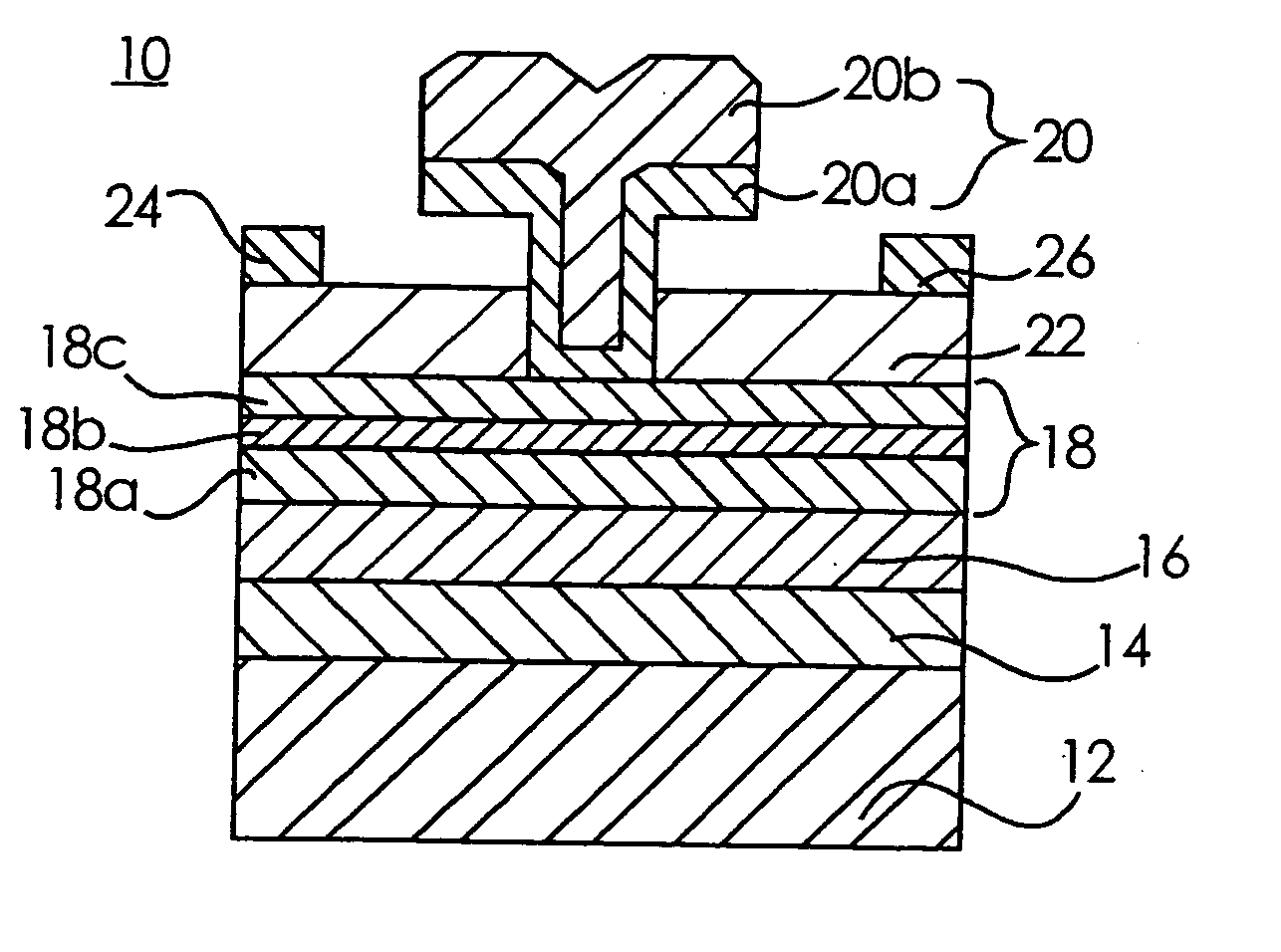
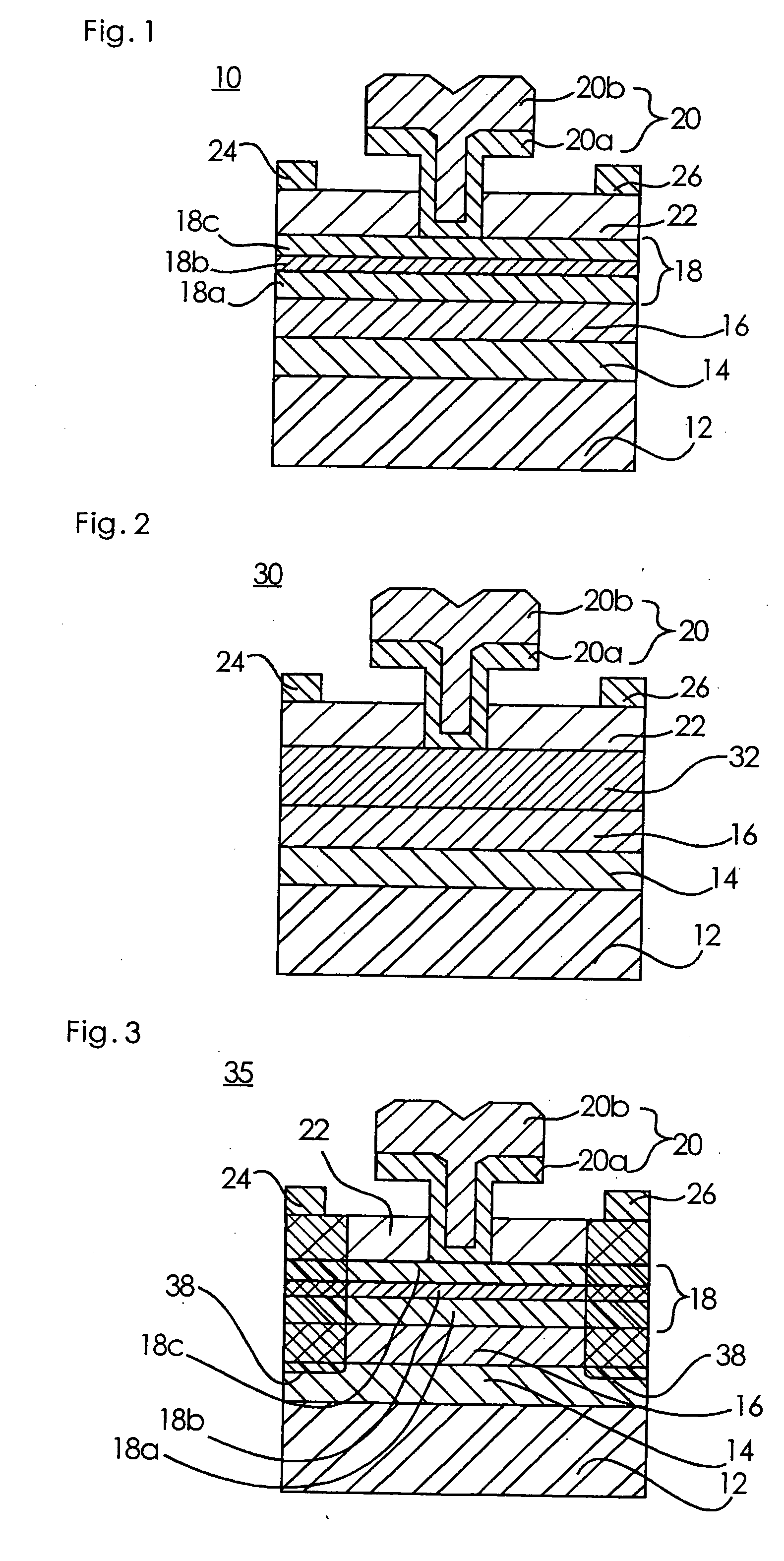
[0027]FIG. 1 is a cross-sectional view of a heterojunction field effect transistor according to an embodiment of the present invention.
[0028]FIG. 1 shows a DCHFET 10 of the first embodiment.
[0029] The DCHFET 10 uses a semi-insulating GaAs substrate 12 serving as a semi-insulating semiconductor substrate. On this GaAs substrate 12, a buffer layer 14 is disposed. The buffer layer 14 is composed of a 450 nm-thick superlattice layer and a 50 nm-thick non-doped GaAs layer disposed thereon. The superlattice layer is formed by depositing a 5 nm-thick GaAs layer and a 5 nm-thick AlGaAs layer repeatedly and alternately on the GaAs substrate 12. (Hereinafter, “i-”, “n-” and “p-” will be used to mean “non-doped”, “n conductivity type”, and “p conductivity type”, respectively.)
[0030] On this buffer layer 14, a 30 nm-thick n-InGaAs layer 16 is disposed serving as a channel layer. This n-InGaAs layer 16 has an impurity concentration of 1×1018 cm−3.
[0031] On this n-InGaAs layer 16, a barrier l...
second embodiment
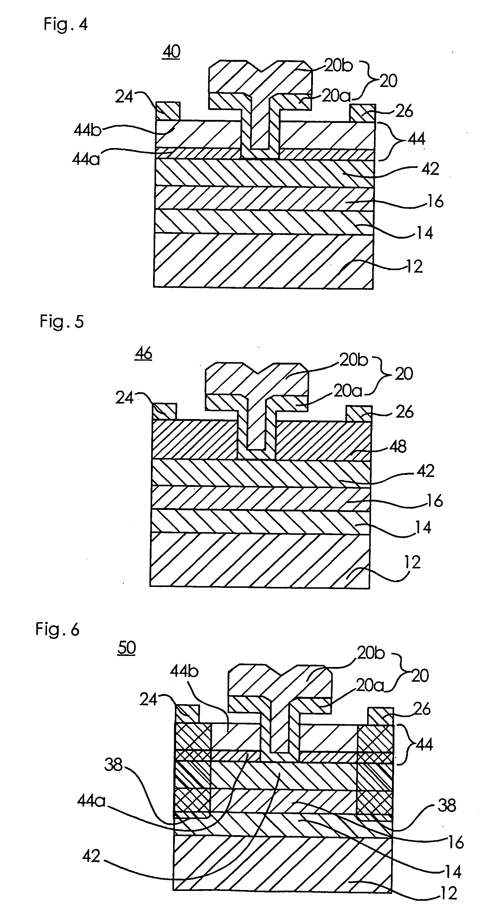
[0059]FIG. 4 is a cross-sectional view of another heterojunction field effect transistor according to another embodiment of the present invention.
[0060]FIG. 4 shows a DCHFET 40 of the heterojunction field effect transistor of the second embodiment. The CHFET 40 is similar to the DCHFET 10 of the first embodiment, but the CHFET 40 is different from the DCHFET 10 in the following two points. First, the barrier layer 42 is composed of a 25 nm-thick i-AlGaAs layer. Second, the 130 nm-thick burying layer 44 disposed on the barrier layer 42 is composed of two layers. The burying layer 44 is composed of a lower burying layer 44a and an upper burying layer 44b. The lower burying layer is in contact with the barrier layer 42 and is composed of a p-GaAs layer, which is substantially fully depleted in thermal equilibrium state. The upper burying layer 44b is composed of an i-GaAs layer. The other elements of the configuration are same as the DCHFET 10 of the first embodiment.
[0061] The lower...
third embodiment
[0082]FIG. 7 is a cross-sectional view of another heterojunction field effect transistor according to another embodiment of the present invention.
[0083]FIG. 7 shows a HEMT 60 of the heterojunction field effect transistor of the third embodiment.
[0084] The HEMT 60 uses a SiC substrate 62 as an insulating substrate. This SiC substrate 62 may be replaced by a sapphire substrate. It is also possible to use a semi-insulating semiconductor substrate. On the SiC substrate 62, an i-GaN layer 64 having a thickness of, for example, 30 nm is disposed as a channel layer. On this i-GaN layer 64, a barrier layer 66 is disposed. In this example of the third embodiment, the barrier layer 66 has a thickness of 30 nm and is composed of an i-Al0.25GaN layer 66a in contact with the i-GaN layer 64, a p-Al0.25GaN layer 66b disposed on the i-Al0.25GaN layer 66a, and an i-Al0.25GaN layer 66c disposed on the p-Al0.25GaN layer 66b. In the thus configured barrier layer 66, the p-Al0.25GaN layer 66b is deple...
PUM
 Abstract
Description
Claims
Application Information


