Gain-clamped semiconductor optical amplifier

a semiconductor optical amplifier and gain-clamped technology, applied in the structure of semiconductor amplifiers, semiconductor lasers, electromagnetic transmission, etc., can solve the problems of deteriorating gain saturation characteristics with respect to signal light, increased current density, and difficulty in achieving high saturated output and polarization independence, so as to reduce the error rate of signal conversion.

Inactive Publication Date: 2013-08-06
NEC CORP
View PDF28 Cites 2 Cited by
  • Summary
  • Abstract
  • Description
  • Claims
  • Application Information

AI Technical Summary

Benefits of technology

[0042]To achieve the above object, a gain-clamped semiconductor optical amplifier according to the present invention has a pair of reflectors disposed in sandwiching relation to a gain area for amplifying guided light, wherein a portion of a waveguide of the gain area comprises a multimode interference optical waveguide. With this arrangement, laser oscillation is caused by the reflectors to clamp a gain in the gain area to an oscillation threshold gain. Therefore, a degradation of a signal waveform due to a gain saturation and interchannel crosstalk upon amplification of wavelength-multiplexed signal light are suppressed. Since the portion of the waveguide of the gain area comprises a multimode interference optical waveguide, the area of the gain area (active layer) is increased, resulting in a corresponding reduction in the density of input light applied to the gain area (active layer) for an increased saturated output.
[0046]The gain-clamped semiconductor optical amplifier may further include a photodetector for detecting the clamped light emitted from the third or fourth port. With this arrangement, if the gain-clamped semiconductor optical amplifier is applied to a repeater amplifier, then the gain-clamped semiconductor optical amplifier operates as described above, and can also operate to produce a constant output by controlling the amount of a current injected into or a voltage applied to the gain adjusting waveguide in order to make the output of the photodetector constant. If the gain-clamped semiconductor optical amplifier is applied to a receiver in an optical communication system, then since the amplified clamped light is detected instead of the signal light, an error rate of signal conversion can be lowered.
[0047]The gain-clamped semiconductor optical amplifier may further include a photodetector for detecting the light emitted from the second port. With this arrangement, the gain-clamped semiconductor optical amplifier operates as described above, and can also lower an error rate of signal conversion.

Problems solved by technology

1) It is difficult to achieve both a high saturated output and polarization independence.
2) The drive current density is increased.
3) The gain saturation characteristics with respect to a signal light are deteriorated.
If the thickness of the active layer is reduced, a crystal strain required for polarization independence will be increased, resulting in crystal growth difficulty.
Therefore, it is difficult to achieve polarization-independent gain characteristics.
However, using such a high current density as a drive condition is not practical in view of deteriorated gain characteristics due to heating and device reliability.
With respect to the factor 3), the saturated output performance on dynamic characteristics for amplifying a modulated signal is not yet sufficient.
This is a problem caused by the definition of a saturated output which serves as an index for estimating the maximum optical output of an SOA.
SOAs, however, cause a signal waveform deterioration when driven in an optical output intensity range with a gain reduction of 3 dB.
Such a signal waveform deterioration is due to the essential nature of SOAs that they are susceptible to a gain saturation relaxation process because the carrier relaxation time in the active layer and the bit rate of the signal light are of about the same order of time.
As described above, it can bee seen that it is highly difficult to achieve a maximum optical output in excess of 20 dBm with the active layer according to the process of optimizing active layer while maintaining the single transverse mode.
In the gain saturation range, since the number of carriers consumed for amplifying the input light increases, the laser-oscillated state cannot be maintained, shutting off the gain clamping operation.
As described above, it is highly difficult to achieve a saturated output of at least 20 dBm mainly through the optimization of the active layer for the following reasons: 1) It is difficult to achieve both a high saturated output and polarization independence.
First, the problems of the process a) of improving the difficulties 1), 2) by increasing the effective waveguide width while maintaining a single transverse mode output will be described below.
It can be seen that because of the drive current, the present process is not sufficient for realizing an SOA which can be used as a substitute for an EDFA.

Method used


Image

  • Gain-clamped semiconductor optical amplifier
  • Gain-clamped semiconductor optical amplifier
  • Gain-clamped semiconductor optical amplifier

Examples


1st embodiment

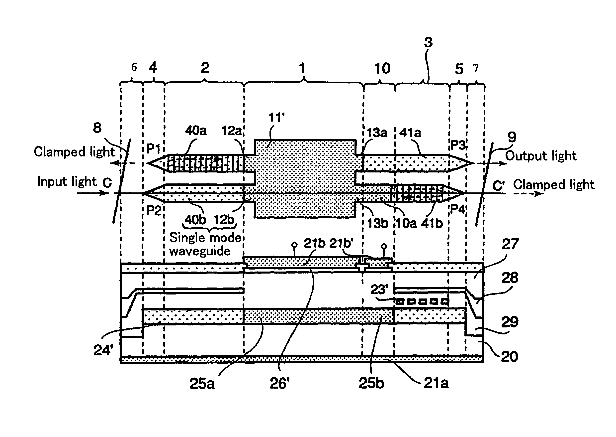
[0093]FIG. 8a is a plan view of a structure of a gain-clamped SOA according to a first embodiment of the present invention, FIG. 8b is a cross-sectional view taken along line C-C′ of the structure shown in FIG. 8a, FIG. 8c is a cross-sectional view taken along line A-A′ of the structure shown in FIG. 8a, and FIG. 8d is a cross-sectional view taken along line B-B′ of the structure shown in FIG. 8a;

[0094]The structure of a waveguide of the gain-clamped SOA according to the present embodiment will be described below with reference to FIG. 8a. As shown in FIG. 8a, the gain-clamped SOA according to the present embodiment has waveguides extending from device end face 8 to which input light is applied to a device end face 9 from which output light is emitted. The waveguides are of a structure having window area 6, SSC (spot size converter) area 4, DBR area 2, gain area 1, DBR area 3, SSC area 5, and window area 7 which are successively arranged from device end face 8. The waveguides close...

experimental example

[0123]The gain saturation performance of the gain-clamped SOA shown in FIGS. 8a through 8d was confirmed by experimentation. First, optical fibers were coupled to device end faces 8, 9 of the gain-clamped SOA, and light having a wavelength of 1.55 μm with a superimposed NRZ modulated signal having a bit rate of 10 Gb / s was applied. When the light intensity of the input signal light was varied at a constant injected current of 700 mA, a constant fiber-to-fiber gain of 20 dB was achieved when the input light intensity was 2 dBm or less. At the same time, it was confirmed that clamped light was being oscillated at a wavelength of 1.51 μm. When a signal error rate of the output signal waveform was measured, no significant increase in the signal error rate as compared with the signal error rate of a signal not passing through the SOA was observed. When the input light intensity was 2 dBm or greater, clamped light stops oscillating, and a reduction in the fiber-to-fiber gain was confirmed...

2nd embodiment

[0126]FIG. 10a is a plan view of a structure of a gain-clamped SOA according to a second embodiment of the present invention, and FIG. 10b is a cross-sectional view taken along line C-C′ of the structure shown in FIG. 10a.

[0127]First, a structure of waveguides of the gain-clamped SOA according to the present embodiment will be described below with reference to FIG. 10a. The gain-clamped SOA according to the present embodiment is basically structurally similar to the gain-clamped SOA shown in FIG. 8a except that a first path through which input light is propagated (a path interconnecting port P2 near device end face 8 and port 3 near device end face 9) and a second path through which clamped light is propagated (a path interconnecting port P1 near device end face 8 and port 4 near device end face 9) are spatially separate from each other. Those structural parts shown in FIG. 10a which are identical to those shown in FIG. 8a are denoted by identical reference characters.

[0128]On the ...


PUM


Abstract

A gain-clamped semiconductor optical amplifier according to the present invention has a pair of DBR areas 2, 3 disposed in sandwiching relation to gain area 1 for amplifying guided light. A portion of a waveguide of gain area 1 comprises MMI waveguide 11.

Description

TECHNICAL FIELD[0001]The present invention relates to a semiconductor optical amplifier, and more particularly to a gain-clamped semiconductor optical amplifier.BACKGROUND ART[0002]Semiconductor optical amplifiers (SOAs) are promising as small-size, low-cost optical amplifiers to replace erbium-doped fiber amplifiers (EDFA) that are typically used in conventional optical communication systems.[0003]One of the goals to be achieved with respect to the performance of SOAs is to increase the saturated output. Generally, the maximum optical output of amplified light generated by SOAs is lower than that of EDFAs. At present, SOAs, which are considered to be more advantageous than EDFAs for their smaller sizes and lower costs, have not been available as a substitute for EDFAs. For SOAs to replace EDFAs in large-capacity wavelength-multiplex optical communication systems, the SOAs need to produce a saturated output of at least 20 dBm (100 mW). In efforts to increase the saturated output, ca...

Claims


Application Information

Patent Timeline
Patent Type & Authority Patents(United States)
IPC IPC(8): H01S4/00H01S5/50H01S5/042
CPCH01S5/0655H01S5/1078H01S5/4068H01S5/5072H01S5/026H01S5/0683H01S5/4025
Inventor HATAKEYAMA, HIROSHI
Owner NEC CORP
Why Eureka
Try Eureka