Circuit device and manufacturing method thereof

a technology of circuit devices and manufacturing methods, applied in the direction of printed element electric connection formation, non-metallic protective coating applications, metal mask etching, etc., can solve the problems of difficult connection parts, limit the size of the integrated circuit, and difficult to form multi-layer wiring structures

Active Publication Date: 2005-12-01
SEMICON COMPONENTS IND LLC
View PDF15 Cites 51 Cited by
  • Summary
  • Abstract
  • Description
  • Claims
  • Application Information

AI Technical Summary

Benefits of technology

[0016] Moreover, the through-hole is provided in the insulating layer which is thinly formed by burying the first connection part. Thus, the through-hole can be easily formed in the insulating layer. Furthermore, since a shallow through-hole can be formed, a plated film can be easily formed in the through-hole....

Problems solved by technology

However, in the hybrid integrated circuit device 100 described above, formation of a single layer of wiring leads to a problem that limits a size of an electric circuit that can be integrated.
However, in the case where a large amount of inorganic fillers are mixed in the ins...

Method used


Image

  • Circuit device and manufacturing method thereof
  • Circuit device and manufacturing method thereof
  • Circuit device and manufacturing method thereof

Examples


first embodiment

[0034] In this embodiment, as an example of a circuit device, a hybrid integrated circuit device as shown in FIGS. 1A to 1C and the like will be described. However, the embodiment described below is also applicable to other kinds of circuit devices. Moreover, the embodiment described below is also applicable to a circuit board and a manufacturing method thereof.

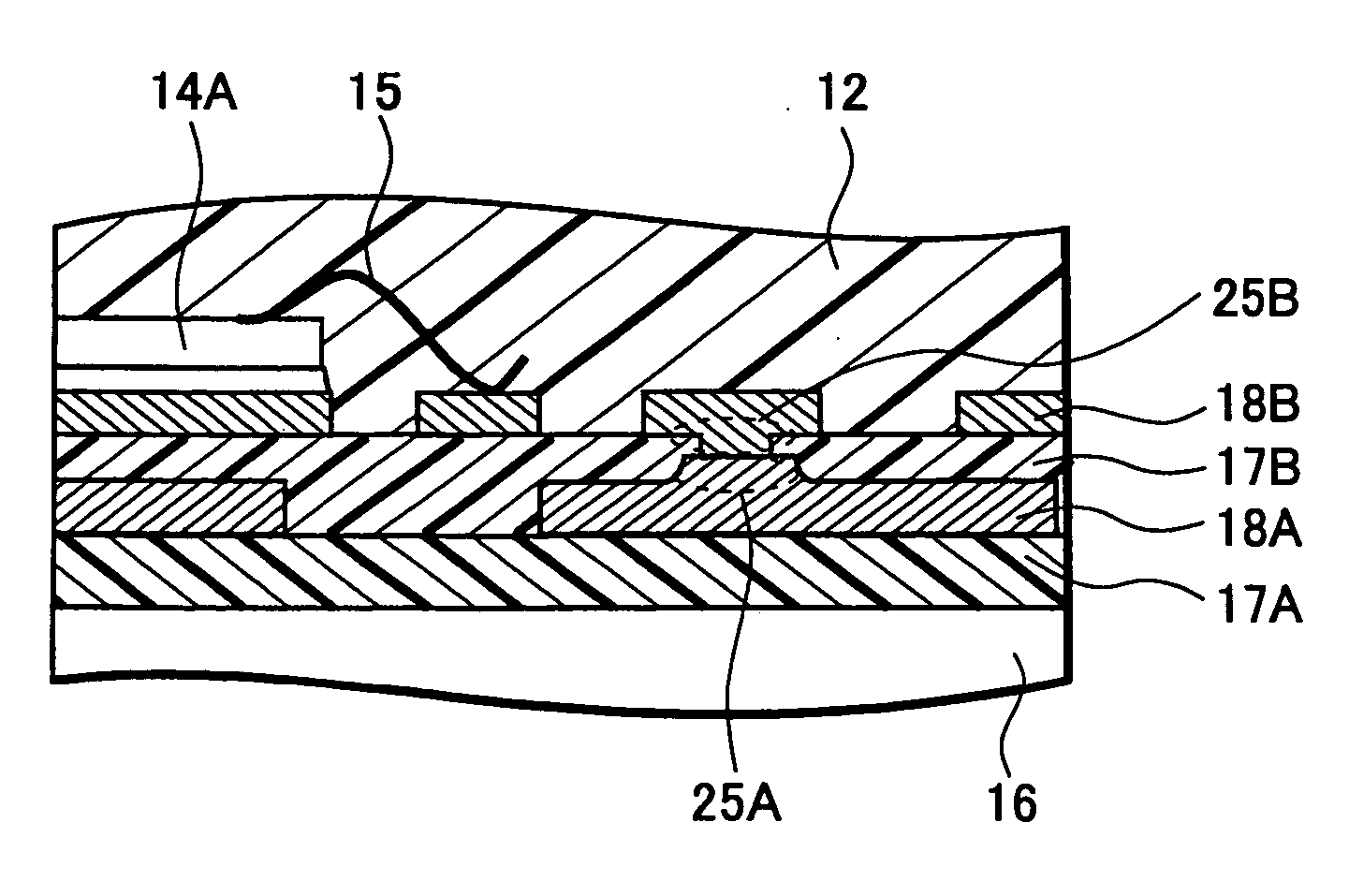
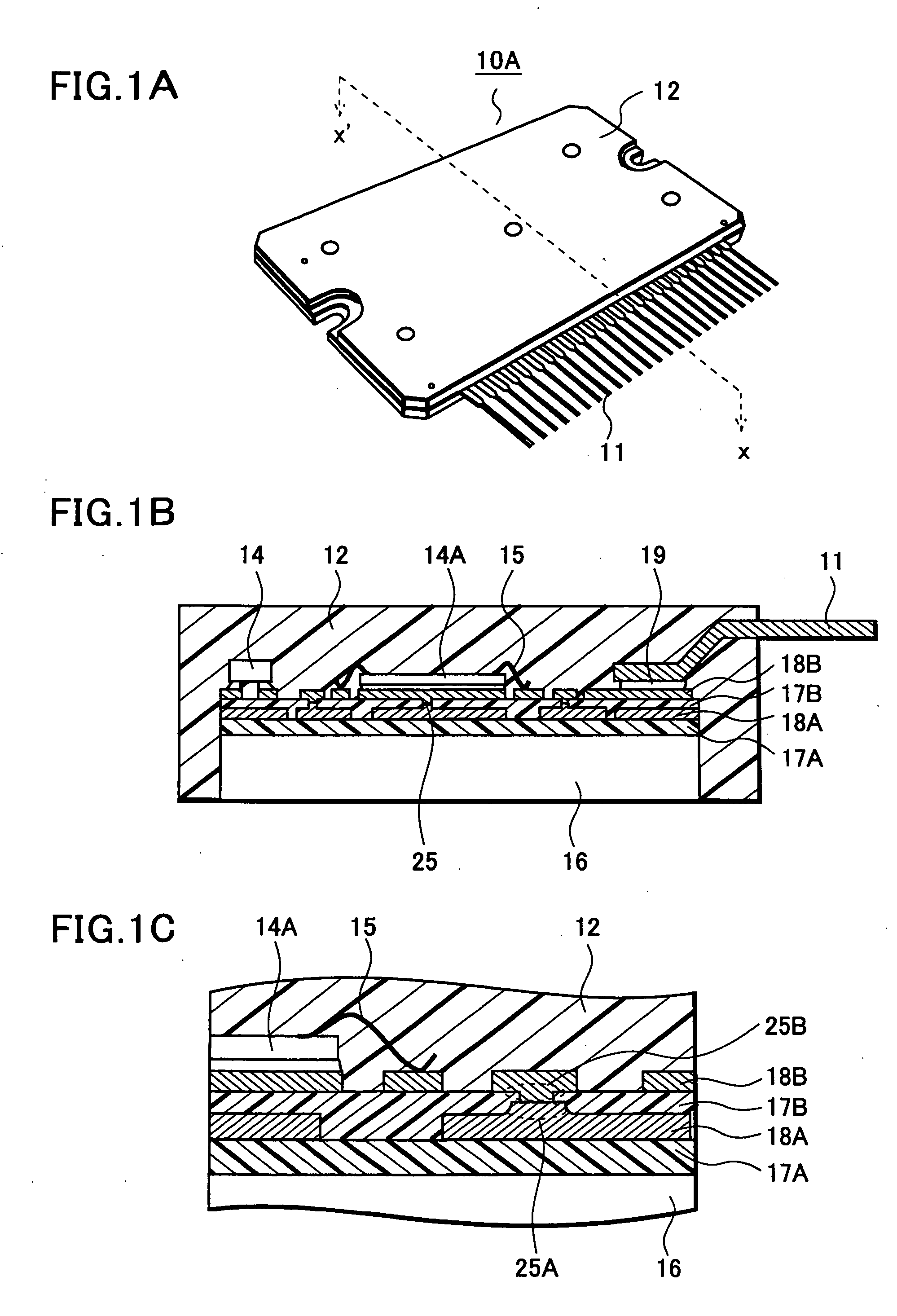
[0035] With reference to FIGS. 1A to 1C, a configuration of a hybrid integrated circuit device 10 according to the embodiment of the present invention will be described. FIG. 1A is a perspective view of the hybrid integrated circuit device 10, and FIG. 1B is a cross-sectional view along the line X-X′ in FIG. 1A. FIG. 1C is an enlarged cross-sectional view around a connection part 25.

[0036] In the hybrid integrated circuit device 10, with reference to FIGS. 1A and 1B, an electric circuit including wiring layers 18 and a circuit element 14 is formed on the surface of a circuit board 16 which functions as a supporting board. M...

second embodiment

[0086] In this embodiment, a description will be given of a method for manufacturing a hybrid integrated circuit device as an example of a circuit device. However, the following manufacturing method of this embodiment is also applicable to methods for manufacturing other types of circuit devices.

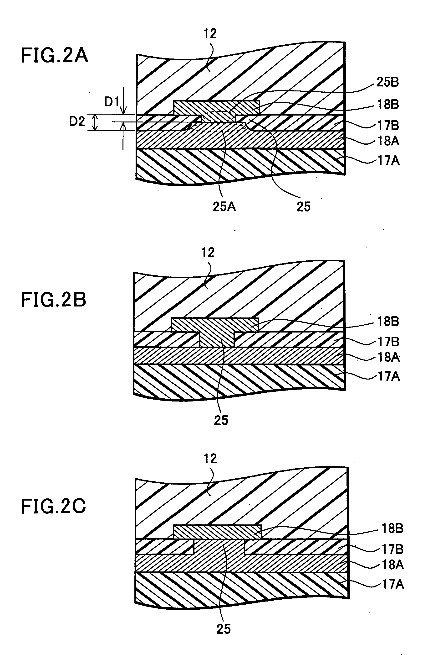
[0087] First, with reference to FIG. 7A, a first insulating layer 17A is applied onto the surface of a circuit board 16, and a first conductive film 28A is laminated thereon. As the circuit board 16, a metal plate having a thickness of about 1.5 mm can be used. Moreover, as the first conductive film 28A, a material mainly made of copper or a material mainly made of Fe—Ni or Al can be used. For a thickness of the first conductive film 28A, not less than a thickness obtained by adding a thickness of a first wiring layer 18A to be formed and a height of a first connection part 25A is required. To be more specific, the thickness of the first conductive film 28A is, for example, about 20 μm to 1...


PUM


Abstract

A circuit device suitable for connecting a plurality of laminated wiring layers to each other through an insulating layer, and a manufacturing method thereof are provided. According to a hybrid integrated circuit device of the present invention and a manufacturing method thereof, a first conductive film is laminated on a first insulating layer, and a first wiring layer is formed by patterning the first conductive film. Next, a second conductive film is laminated on a second insulating layer. Thereafter, by partially removing the second insulating layer and the second conductive film in a desired spot, a connection part for connecting the wiring layers to each other is formed.

Description

BACKGROUND OF THE INVENTION [0001] Priority is claimed to Japanese Patent Application Number JP2004-162652 filed on May 31, 2004, the disclosure of which is incorporated herein by reference in its entirety. [0002] 1. Field of the Invention [0003] The present invention relates to a circuit device and a manufacturing method thereof, and more particularly relates to a circuit device including a plurality of wiring layers laminated with an insulating layer interposed therebetween, and a manufacturing method thereof. [0004] 2. Description of the Related Art [0005] With reference to FIGS. 16A and 16B, a description will be given of a configuration of a conventional hybrid integrated circuit device 100. This technology is described for instance in Japanese Patent Application Publication No. Hei 6 (1994)-177295. FIG. 16A is a perspective view of the hybrid integrated circuit device 100, and FIG. 16B is a cross-sectional view along the line X-X′ in FIG. 16A. [0006] The conventional hybrid in...

Claims


Application Information

Patent Timeline
IPC IPC(8): H05K1/11H01L21/48H01L23/12H01L23/31H01L23/48H01L23/498H01L23/538H01L25/04H01L25/18H05K1/05H05K3/00H05K3/28H05K3/40H05K3/42H05K3/46
CPCH01L21/4857H01L2924/1301H01L23/49822H01L23/5383H01L24/97H01L2221/68377H01L2224/16225H01L2224/32225H01L2224/48091H01L2224/48227H01L2224/48472H01L2224/73204H01L2224/73253H01L2224/73265H01L2224/97H01L2924/01012H01L2924/01013H01L2924/0102H01L2924/01029H01L2924/0103H01L2924/01033H01L2924/01046H01L2924/01047H01L2924/01078H01L2924/01079H01L2924/01082H01L2924/19041H01L2924/19105H01L2924/19107H05K1/056H05K3/0035H05K3/284H05K3/421H05K3/423H05K3/4647H05K3/4652H05K2201/0209H05K2201/09563H05K2201/096H05K2203/0369H05K2203/0554H05K2203/1476H01L23/3121H01L2924/07802H01L2924/10253H01L24/48H01L2924/01005H01L2924/01006H01L2924/01019H01L2924/13055H01L2924/00014H01L2224/85H01L2924/00H01L2924/00012H01L2224/92247H01L2224/451H01L2924/351H01L2924/12042H01L24/45H01L2924/14H01L2924/181H01L24/49H01L2224/4903H01L2924/16152H01L2224/05599H01L23/50
Inventor IGARASHI, YUSUKENAKAMURA, TAKESHIINOUE, YASUNORIMIZUHARA, HIDEKIUSUI, RYOSUKE
Owner SEMICON COMPONENTS IND LLC
Why Eureka
Try Eureka