Shift register

a technology of shift register and shift register, which is applied in logic circuits, pulse techniques, instruments, etc., can solve the problems of shift register operation and inability of amorphous silicon thin film transistors to function properly

Active Publication Date: 2005-12-01
LG DISPLAY CO LTD
View PDF3 Cites 140 Cited by
  • Summary
  • Abstract
  • Description
  • Claims
  • Application Information

AI Technical Summary

Benefits of technology

[0023] An advantage of the present invention is that it enables a shift register to be fabricated with amorphous silicon.
[0024] Another advantage of the present invention is that it enables a shoft register to be integrated into an LCD panel.
[0025] Additional advantages of the invention will be set forth in the description which follows, and in part will be apparent from the description, or may be learned by practice of the invention. The advantages of the invention will be realized and attained by the structure particularly pointed out in the written description and claims hereof as well as the appended drawings.
[0026] The aforementioned and other advantages of the present invention are achieved with a shift register having a plurality of stages that comprises first, second, and third driving voltage supply lines; at least two clock signal supply lines; an output buffer having an output pull-up transistor and a first and second output pull-down transistors; a first controller having an input connected to a start signal supply line and an output connected to a first node; and a second controller having an input connected to the first and second voltage supply lines and an output connected to the gates of the first and second output pull-down transistors.
[0027] In another aspect of the present invention, the aforementioned and other advantages are achieved by a shift register having a plurality of stages that comprises an output buffer having first transistor and an even and odd transistor, the even and odd transistors having the same polarity a first controller for controlling a state of the output buffer; and a second controller for switching between the even and odd transistor.

Problems solved by technology

However, the amorphous silicon thin film transistor may not function properly due to bias stress when a direct current voltage DV is continuously supplied to the thin film transistor's gate terminal.
Therefore, a problem arises in that an erroneous operation of the shift register, such as a multiple output generation, occurs below a certain voltage on the QB node.

Method used


Image

  • Shift register
  • Shift register
  • Shift register

Examples


Embodiment Construction

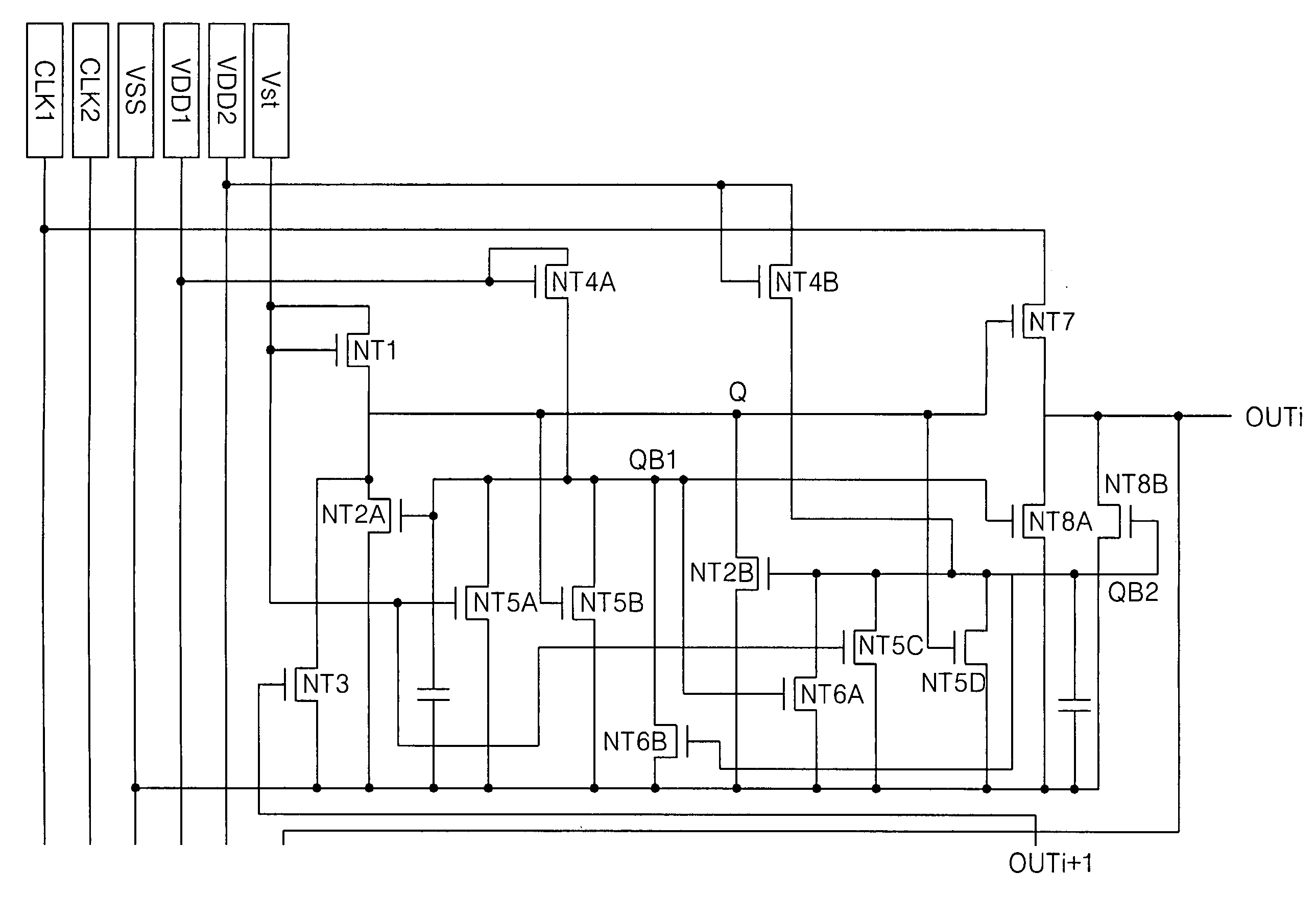
[0035] Reference will now be made in detail to the illustrated embodiments of the present invention. Hereinafter, the illustrated embodiments of the present invention will be described with reference to FIGS. 4 and 5.

[0036]FIG. 4 is a circuit diagram illustrating a configuration of any one of a plurality of stages connected in cascade in a shift register according to an embodiment of the present invention. FIG. 5 is a driving waveform diagram of a stage illustrated in FIG. 4.

[0037] Referring to FIG. 4, a stage of the shift register includes an output buffer having a pull-up transistor NT7 for outputting a first clock signal CLK1 to an output line under control of a Q node, and first and second pull-down transistors NT8A and NT8B for outputting a third driving voltage VSS to the output line under control of QB1 and QB2 nodes; a first controller having first to third transistors NT1 to NT3 for pre-charging and discharging the Q node; and a second controller having transistors NT4A t...


PUM


Abstract

Disclosed is a shift register capable of mitigating gate bias stress. The shift register, including a plurality of stages, includes an output buffer having a pull-up transistor and two pull-down transistors, each with gates connected to different nodes. One of the two pull-down transistors operates during an even frame portion of an LCD operation; and the other of the two pull-down transistors operates during an odd frame portion of the LCD display operation. Alternating operation of the pull-down transistors substantially mitigates gate stress, and substantially enables the shift register to be fabricated with amorphous silicon.

Description

[0001] This application claims the benefit of Korean Patent Application No. P2004-39136 filed in Korea on May 31, 2004, which is hereby incorporated by reference BACKGROUND OF THE INVENTION [0002] 1. Field of the Invention [0003] This invention relates to a driving circuit for a liquid crystal display, and more particularly to a shift register employing an amorphous silicon thin film transistor. [0004] 2. Discussion of the Related Art [0005] Generally, a liquid crystal display (LCD) used as a display device for a television or a computer controls light transmittance of a liquid crystal using an electric field. To this end, the LCD includes a liquid crystal display panel having liquid crystal cells arranged in a matrix, and a driving circuit for driving the liquid crystal display panel. [0006] In the liquid crystal display panel, gate lines and data lines are arranged in such a manner to cross each other. The crossing gate lines and data lines define a plurality of liquid crystal cel...

Claims


Application Information

Patent Timeline
Patent Type & Authority Applications(United States)
IPC IPC(8): H03K19/00G09G3/36G11C19/00G11C19/28
CPCG09G2300/0408G11C19/28G11C19/184G11C19/00H03K19/00
Inventor KIM, BINNYOON, SOO YOUNG
Owner LG DISPLAY CO LTD
Why Eureka
Try Eureka