Liquid crystal display apparatus
- Summary
- Abstract
- Description
- Claims
- Application Information
AI Technical Summary
Benefits of technology
Problems solved by technology
Method used
Image
Examples
first embodiment
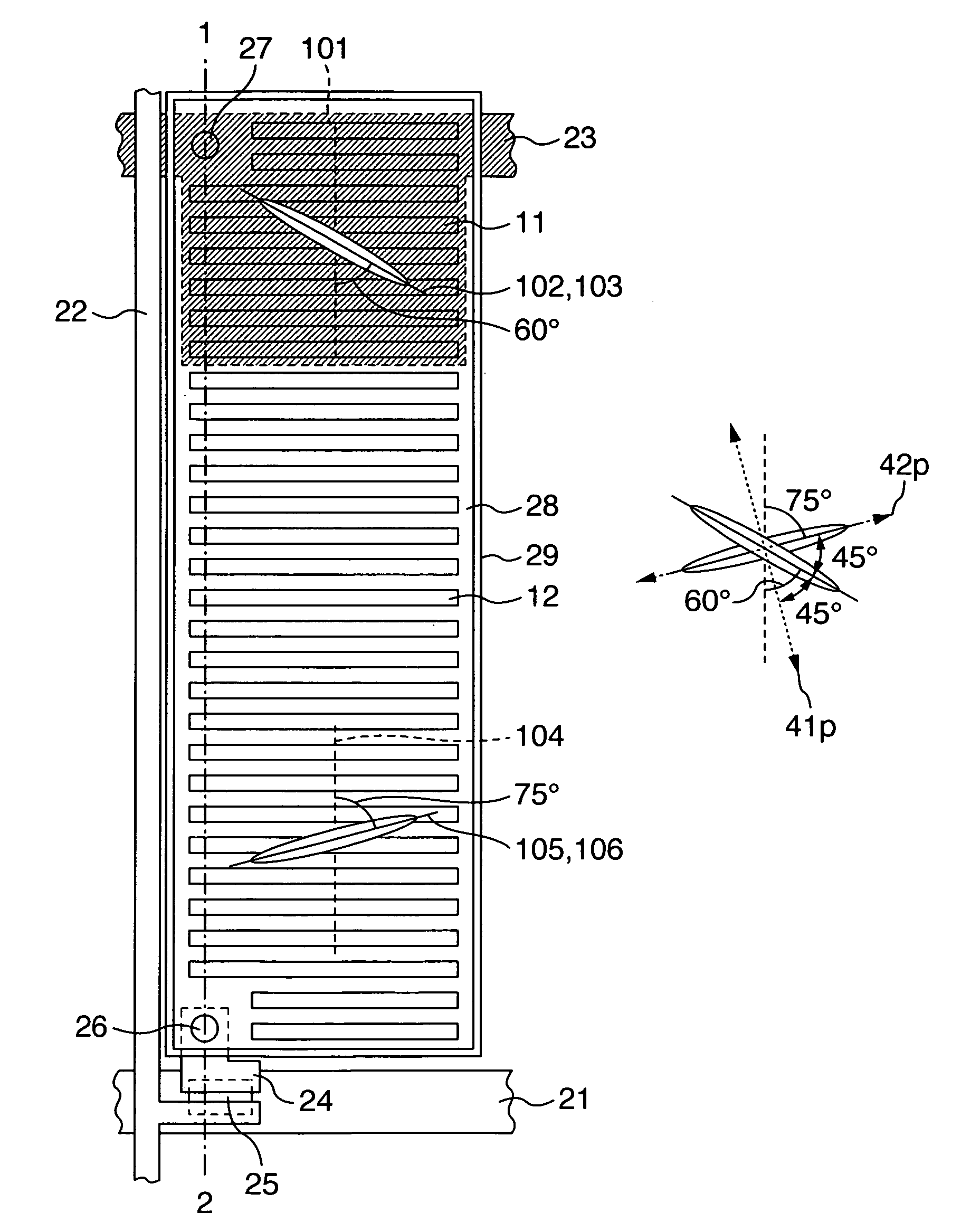
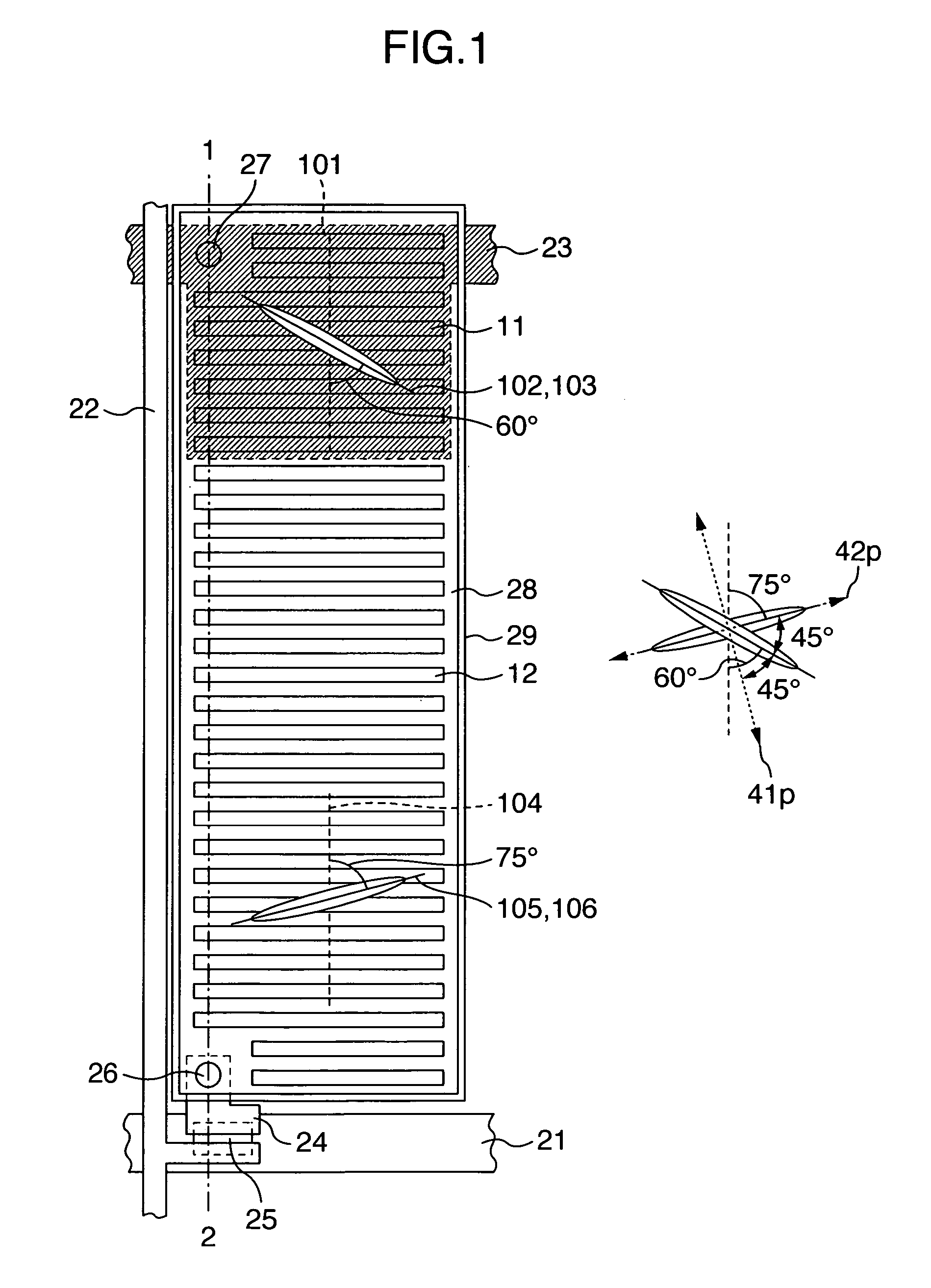
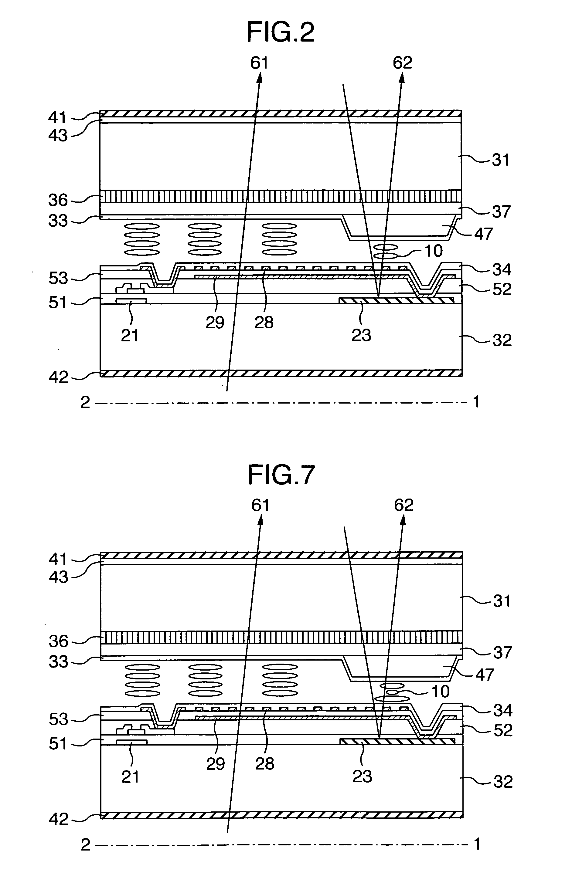
[0052] A section of one of the pixels composing the liquid crystal display (referred to as LCD) apparatus according to the present invention is illustrated in FIG. 2. A top view of a second substrate 32 shown in the section of FIG. 2 is illustrated in FIG. 1, in which view the second substrate 32 is observed from the normal direction. The section of FIG. 1 on a dashed line 1-2 corresponds to FIG. 1. As shown in FIG. 2, the LCD apparatus according to the present invention is mainly composed of a first substrate 31, a liquid crystal layer 10 and the second substrate 32, in which apparatus the liquid crystal layer 10 is laid between the first and the second substrates 31 and 32.
[0053] The first substrate 31 includes a color filter 36, a leveling layer 37 and a first alignment layer 33 on the side closer to the liquid crystal layer 10. The second substrate 32 includes a thin film transistor on the side closer to the liquid crystal layer 10. The thin film transistor is connected with a ...
second embodiment
[0088] In the first embodiment, the reflective display portion has the different alignment direction of the liquid crystal from the transmissive display portion. Hence, in both of the first and the second alignment layers 33 and 34, the reflective display portion and the transmissive display portion are respectively treated by the rubbing technique with a mask. This treatment results in increasing the steps of the manufacturing process.
[0089] The alignment direction and the liquid crystal alignment state in the reflective display portion and the transmissive display portion of the LCD apparatus according to this embodiment are shown in FIG. 6. In this embodiment, only the first alignment layer 33 is differently aligned between the reflective display portion and the transmissive display portion. The second alignment layer 34 is uniformly aligned on the overall surface. This results in reducing the steps of the manufacturing process. That is, like the first embodiment, for the first ...
third embodiment
[0096] The top view of the LCD apparatus according to this embodiment is shown in FIG. 9. In this embodiment, each of the pixel electrode 28 and the common electrode 29 is formed in a combshaped manner and both of the electrodes are formed in the same layer. This makes it possible to form the arched electric field between the pixel electrode 28 and the common electrode 29 when a voltage is applied, thereby causing the electric field to drive the liquid crystal layer.
[0097] The combshaped structure of each electrode 28 or 29 is formed in parallel to the signal electrode 22 in any of the reflective display portion and the transmissive display portion. Hence, the electric field direction 101 of the reflective display portion and the electric field direction 104 of the transmissive display portion are vertical to the signal electrode 22. In association with this direction, the alignment directions of the reflective display portion and the transmissive display portion were set as shown ...
PUM
 Abstract
Description
Claims
Application Information


