Memory system for an electronic device and the method for controlling the same

a technology of electronic devices and memory systems, applied in the field of memory systems, can solve the problems of poor programming and erasing speed, less flexibility of the system designer, and increased cost difference between the two kinds of memories, and achieve the effect of fast system startup time and low bit error ra

Inactive Publication Date: 2005-12-01
KUAN PETER +1
View PDF7 Cites 20 Cited by
  • Summary
  • Abstract
  • Description
  • Claims
  • Application Information

AI Technical Summary

Benefits of technology

[0014] The objective of the present invention is to provide a unique memory system for electronic devices, wherein the data flash memory and code flash memory are integrated together thus simultaneously possessing the advantages (such as fast system startup time, low bit error rate, and emergency recovery data) of these two different types of memories.

Problems solved by technology

This kind of memory design may be the simplest method, but it is also the least flexible for the system designer when it becomes necessary to expand the memory capacity.
Further, although NOR flash memory possesses the eXecute In Place (XIP) function, its programming and erasing speed is quite poor compared with the data flash memory (e.g., NAND flash memory).
Moreover, because NOR flash memory uses linear addressing design, every memory cell must function normally, i.e., no memory cell can be permitted to have bad data.
With the ever-increasing requirements for high-capacity memory, the cost difference between the two kinds of memories has become more apparent.
Such a high RC value usually leads to a longer data accessing time and is unfavorable to the entire system efficiency.
After system startup, a bit error may possibly occur when a great quantity of data is accessed or erased.
Since all kinds of data—including binary execute boot code (103), OS (104), and user data (105)—are stored in the same code flash memory (101), the bit error may cause critical damage.
For example, it is possible that when intending to erase user data (105), abnormal level status on the address lines may cause the boot code (103) to be accidentally erased instead.
As mentioned above, a large RC value may lead to long data reading, writing, and erasing times. The high RC value would thus increase the possibility of bit errors since the Bit Error Rate (BER) is in direct proportion to the data accessing time.
That is because data can only be successfully written to or erased from data flash memory by writing or erasing the correct data several times in succession.
However, since the data flash memory design employs the “multi-function pins” technique, it is unable to provide a binary execute boot code during the system startup.
This data transfer procedure needs a long time and thus may cause a serious delay to the subsequent initializing of the display device.
Further, when an unexpected writing action occurs in a critical data area of the data flash memory, the system may not be able to be booted any more.
In short, it is difficult to provide a reliable memory system using a single data flash memory and even when done so, it involves a long startup time.

Method used


Image

  • Memory system for an electronic device and the method for controlling the same
  • Memory system for an electronic device and the method for controlling the same
  • Memory system for an electronic device and the method for controlling the same

Examples


Embodiment Construction

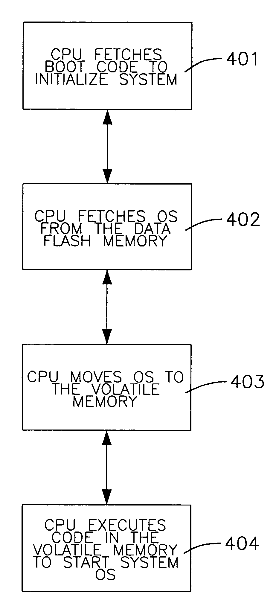
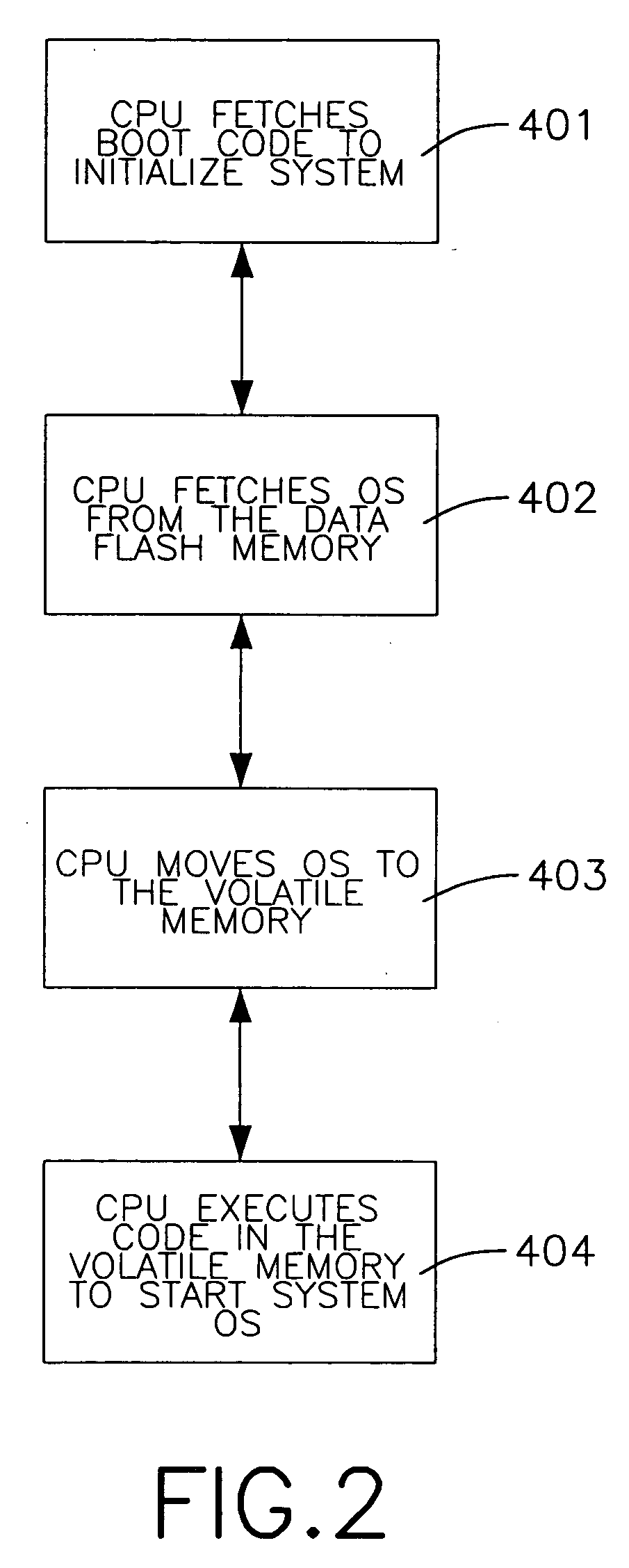
[0024] As discussed in the prior art, data flash memory and code flash memory both possess their respective advantages and limitations; however, data flash memory is still superior to code flash memory in the aspects of extended capacity and data reading / writing reliability. Although the system is unable to directly retrieve the boot code from the data flash memory, using code flash memory of a small capacity can solve the problem. The present invention thus integrates the foregoing two types of memories as a unique memory system and is applied for use in electronic products.

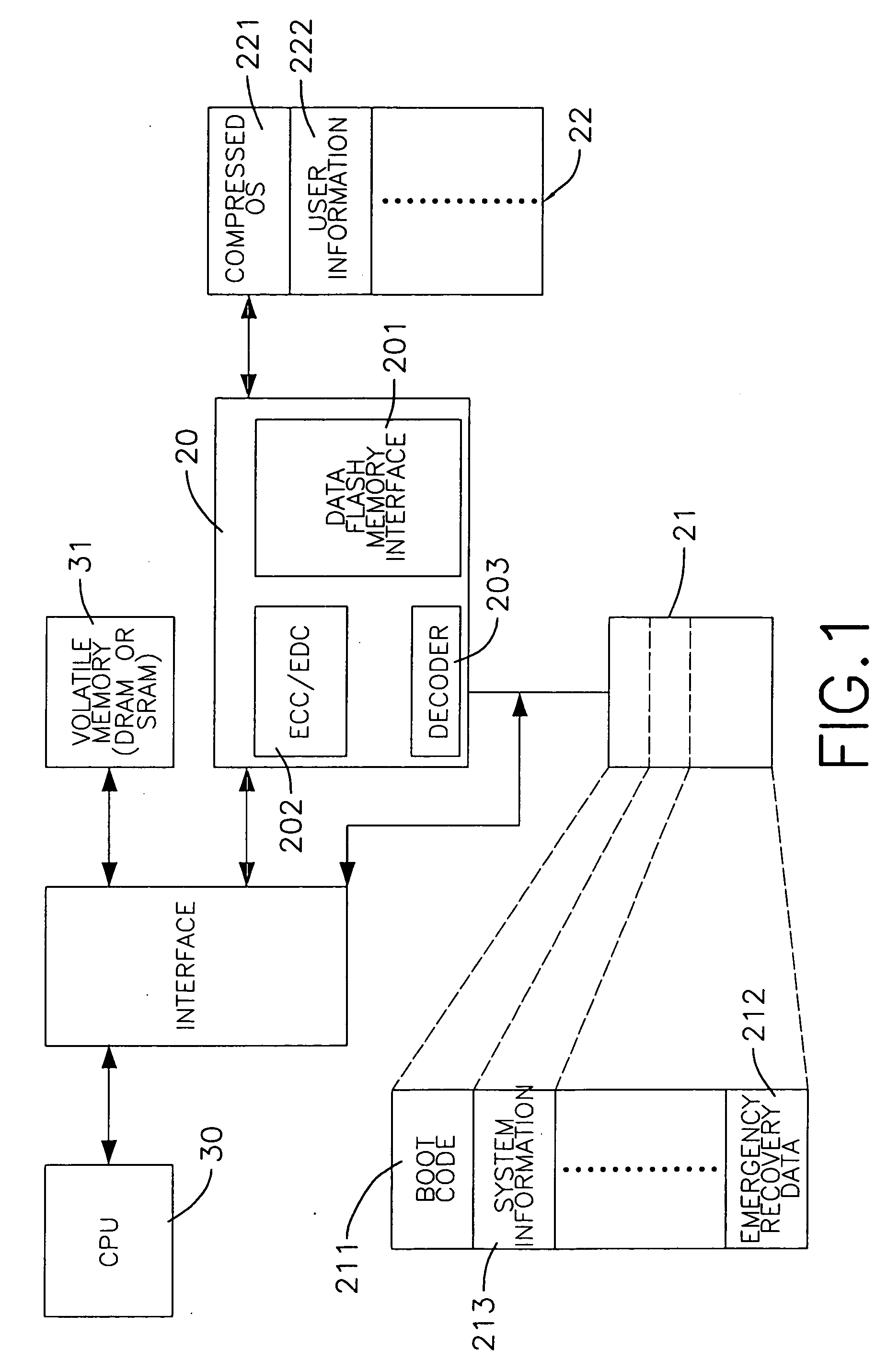
[0025] With reference to FIG. 1, the memory system according to the present invention is applied in an electronic device (for example, a cell phone or PDA), and comprises a control unit (20), linear-addressing nonvolatile memory (21), and data flash memory (22).

[0026] The control unit (20) couples to a CPU (30) of the electronic device through an interface (not numbered), wherein volatile memory (31) such as a...


PUM


Abstract

A memory system applied to an electronic device has a small-capacity linear-addressed nonvolatile memory having a boot code and system information stored therein and a high-capacity data flash memory in which an operating system (OS) and frequently accessed user data are recorded. While the memory system is booting up, the boot code including the system information is fetched from the linear-addressed nonvolatile memory to start an initialization process. After completion of the initialization process, the OS is retrieved from the data flash memory and executed. During the OS retrieval, the memory system provides an ECC/EDC unit to detect whether any bit error occurs and to correct any if present. Since the boot code and OS are stored in different memories, the bit error rate (BER) is effectively reduced.

Description

BACKGROUND OF THE INVENTION [0001] 1. Field of the Invention [0002] The present invention relates to a memory system applied for an electronic device, more particularly, the memory system utilizes a small linear addressing nonvolatile memory in company with a controller to control a high-capacity data flash memory. [0003] 2. Description of Related Art [0004] The traditional memory system design for mobile phone or PDA systems usually employs code flash memory (e.g., NOR flash memory). Code flash memory consists of blocks designated to store the system boot code, the operating system (OS), and user data. This kind of memory design may be the simplest method, but it is also the least flexible for the system designer when it becomes necessary to expand the memory capacity. Limited by the linear addressing of the NOR flash memory, the entire memory system hardware must be changed in order to extend the data storage capacity. Further, although NOR flash memory possesses the eXecute In Pl...

Claims


Application Information

Patent Timeline
Patent Type & Authority Applications(United States)
IPC IPC(8): G06F9/00G06F9/445
CPCG06F9/4406
Inventor KUAN, PETERHU, TA-SHIN
Owner KUAN PETER
Why Eureka
Try Eureka