Optical sensor, output processing method of optical sensor, display device, and electronic apparatus

US20050269486A1Active Publication Date: 2005-12-08138 EAST LCD ADVANCEMENTS LTD

Image

  • Optical sensor, output processing method of optical sensor, display device, and electronic apparatus
  • Optical sensor, output processing method of optical sensor, display device, and electronic apparatus
  • Optical sensor, output processing method of optical sensor, display device, and electronic apparatus

Examples


first embodiment

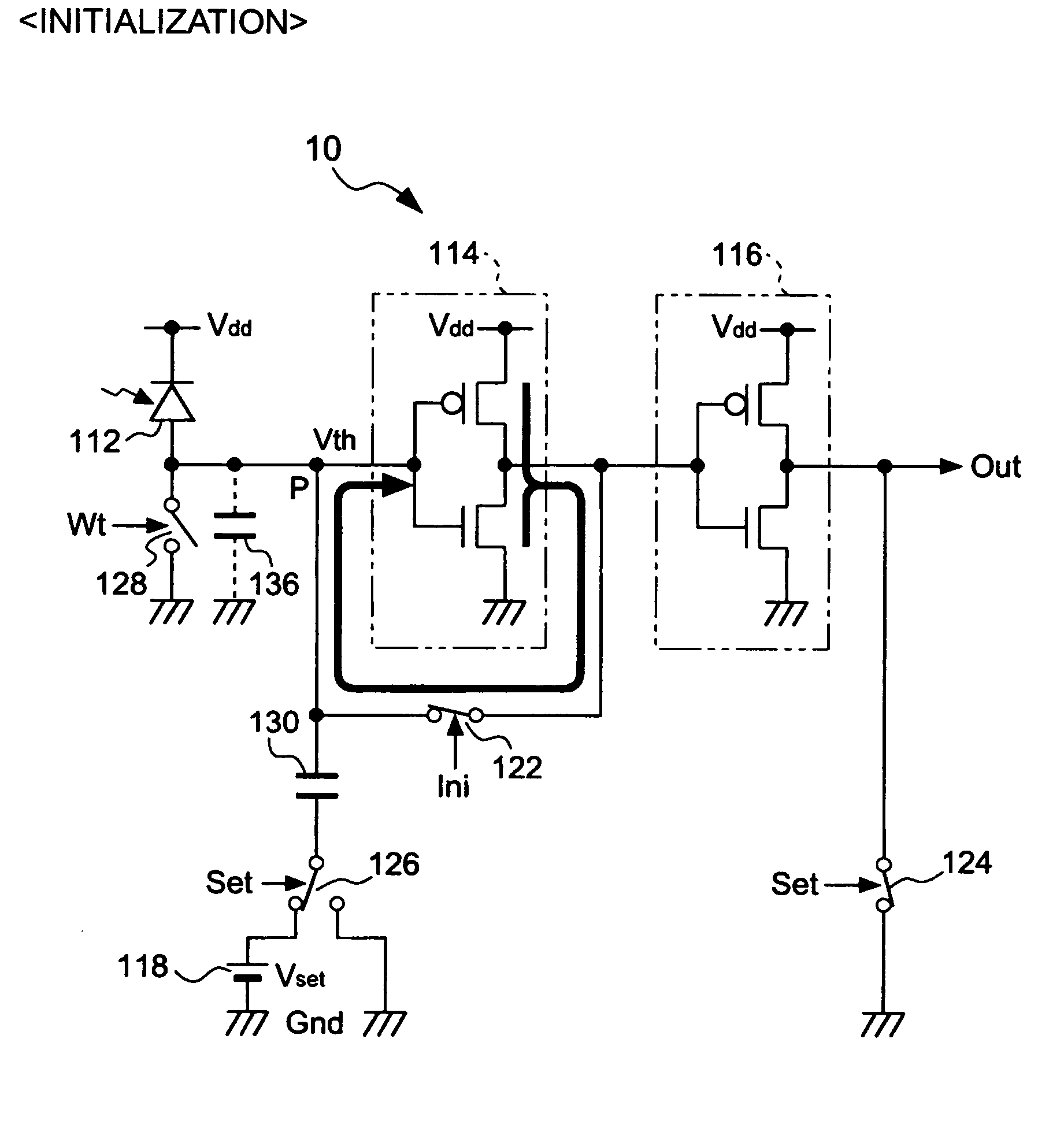
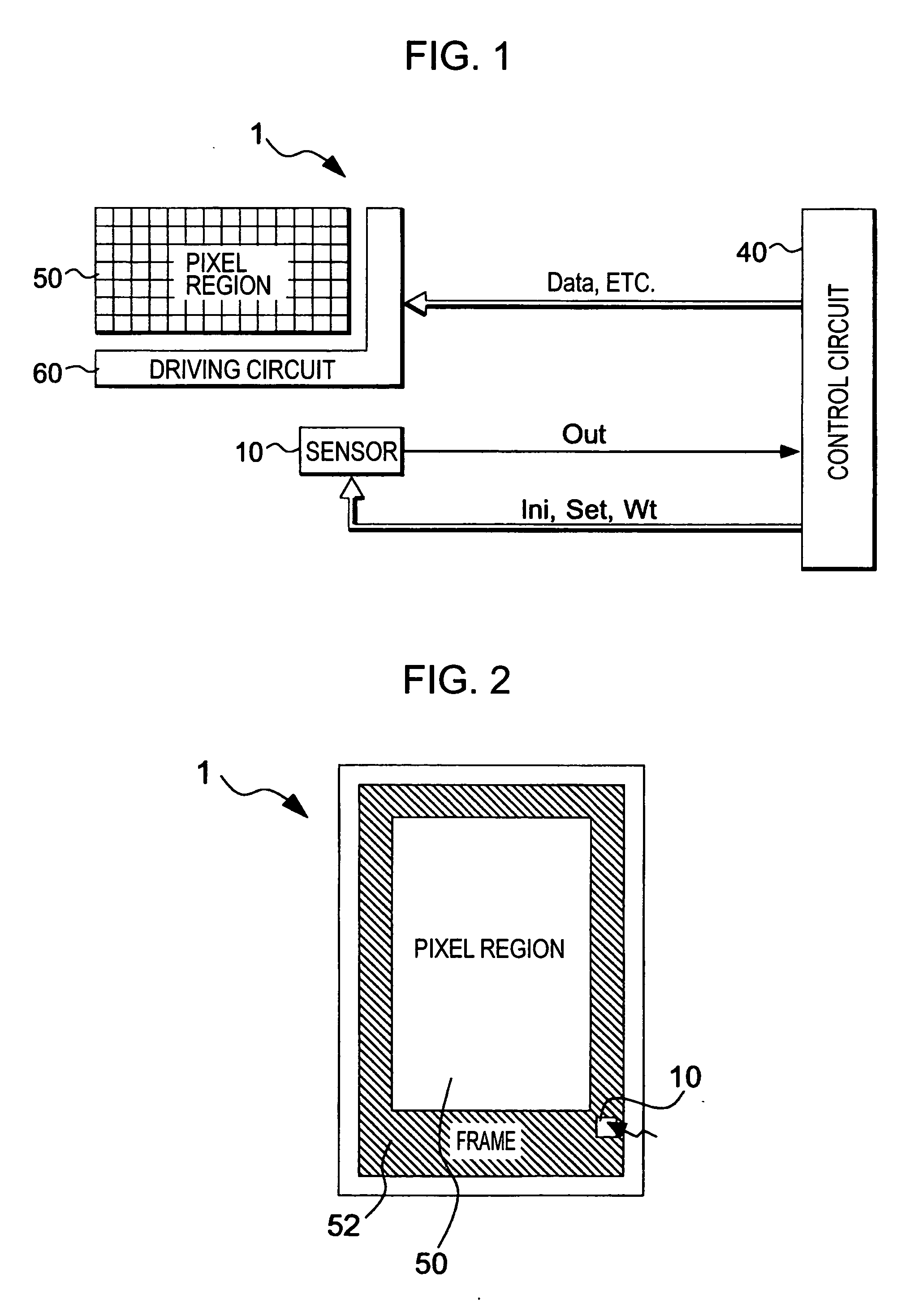
[0034]FIG. 1 is a block diagram showing the overall structure of a display panel including an optical sensor according to a first embodiment of the invention.

[0035] In FIG. 1, an optical sensor 10 outputs a signal Out according to the amount of received light, which will be described later in detail. According to the present embodiment, as the amount of the received light increases, the pulse width of the signal Out is narrowed.

[0036] As shown in FIG. 2, the optical sensor 10 is provided right below a frame (light shielding layer) 52 which defines an outer circumference of a pixel region 50. In addition, a light receiving surface of the optical sensor 10 is located at a part of the frame 52 where an opening is formed.

[0037] In addition, the pixel region 50 is a region where a plurality of pixels is arranged in a matrix.

[0038] Assuming that the display panel 1 is a liquid crystal panel, the pixels are respectively arranged so as to correspond to intersections of scanning lines an...

second embodiment

[0083] On the other hand, as described above, in the structure in which any one of the plurality of voltages is selected as the voltage Vset according to the state of the signal Out, a plurality of different voltages must be previously prepared, and it must be considered that the structure of the power supply circuit (voltage generating circuit) (not shown) becomes complicated. Therefore, the optical sensor using one kind of voltage Vset while preventing the information according to the received light amount from not being obtained will be described with reference to a second embodiment.

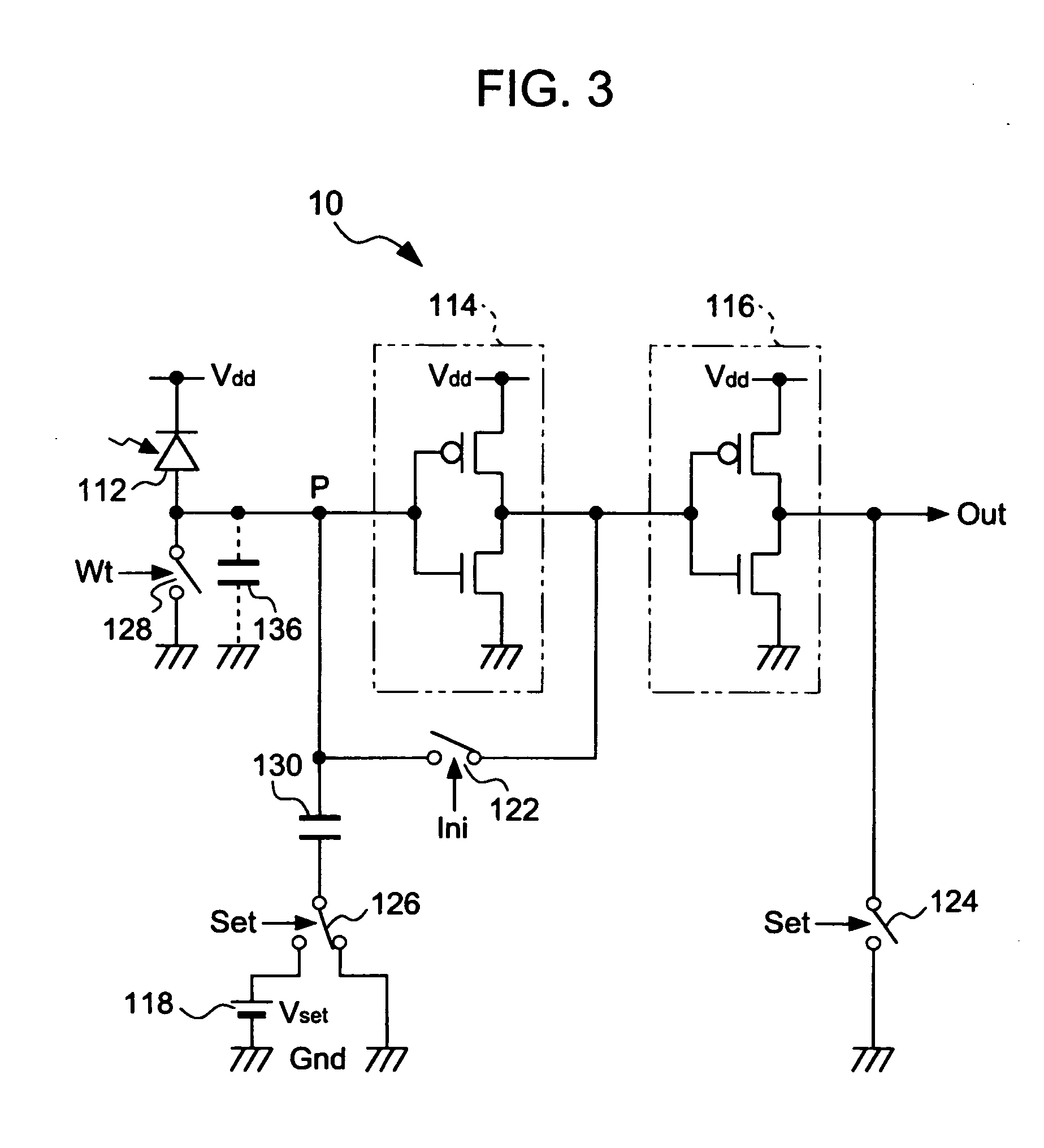
[0084]FIG. 11 is a diagram showing the structure of an optical sensor 10 according to the second embodiment of the invention.

[0085] The optical sensor 10 according to the second embodiment shown in FIG. 11 is the same structure as that in the first embodiment, except that the capacitor element 130 shown in FIG. 3 is replaced with a portion shown by a region Q. Therefore, only the different structur...


PUM


Abstract

An optical sensor includes a light receiving element in which a current corresponding to the amount of received light flows between one end and the other end thereof, a comparator which compares a voltage at the one end of the light receiving element with a predetermined threshold voltage to output a logical signal based on the comparison result, an initialization circuit which initializes the voltage at the one end of the light receiving element to the threshold value or a voltage approximate to the threshold voltage before detecting the amount of the received light, and a voltage changing circuit which changes the voltage at the one end of the light receiving element by a predetermined voltage after completing the initialization. In the optical sensor, after changing the voltage by the voltage changing circuit, a period until the logical signal output from the comparator is logically inverted is expressed as a value corresponding to the amount of the received light.

Description

BACKGROUND OF THE INVENTION [0001] 1. Technical Field [0002] The invention relates to a technology for reading out the output of a light-receiving element, such as a photodiode. [0003] 2. Related Art [0004] In recent years, display panels in which liquid crystal elements or organic EL (electroluminescent) elements are arranged in a matrix in electronic apparatuses, such as cellular phones and PDAs (personal digital assistants) have been widely spread. Such a display panel is used in various environments from a bright state to a dark state. For this reason, when the brightness or image quality of a display element is uniform irrespective of external light, it is easy for a user to see a display screen in any environment. On the other hand, it is very difficult for the user to see the display screen in other environments. Therefore, in the display panel, it is required that the amount of external light be detected and that the brightness or image quality of a display image be controll...

Claims


Application Information

Patent Timeline
08 Dec 2005
Publication
US20050269486A1
IPC
G01J1/18; G01J1/46; G01J1/42; G02F1/133; G09G3/20; H01J40/14; H01L27/146; H01L31/10
CPC
G01J1/46; G01J1/18; H01L31/10
Inventors
OZAWA, TOKURO