
Fin field effect transistors and methods of fabricating the same

a transistor and field effect technology, applied in the field of semiconductor devices, can solve the problems of abnormal transistor operation, effect and dibl effect, and large threshold voltage variation depending on the threshold voltag

Active Publication Date: 2005-12-08
SAMSUNG ELECTRONICS CO LTD
View PDF2 Cites 92 Cited by
  • Summary
  • Abstract
  • Description
  • Claims
  • Application Information

AI Technical Summary

Benefits of technology

[0010] In some embodiments of the present invention, a fin field effect transistor (FinFET) includes a substrate, a fin, a gate electrode, a gate insulation layer, and source and drain regions in the fin. The fin is on and extends laterally along and vertically away from the substrate. The gate electrode covers sides and a top portion of the fin. The gate insulation layer is between the gate electrode and the fin. The source region and the drain region are in the fin and adjacent to opposite sides of the gate electrode. The source region of the fin has a different width than the drain region of the fin.

Problems solved by technology

The continuing trend to fabricate semiconductor devices with smaller device features has led to some difficulties when trying to scale-down transistors that have a horizontal channel (hereinafter referred to as “horizontal channel transistors”).
Two difficulties that can arise when trying to scale-down horizontal channel transistors are short channel effect and drain induced barrier lower (DIBL) effect.
When the channel length is 30 nanometers or less, the channel effect and DIBL effect can become so severe that the resulting transistor will operate abnormally.
One difficulty in using FinFETs is that threshold voltages can vary considerably depending upon variations in their fabrication processes.
Consequently, it can be difficult to control the threshold voltage of the transistor and provide cell uniformity in a high-density memory device.
Lowering of the threshold voltage of a transistor can increase the sub-threshold voltage leakage.
Leakage current of a transistor results in degradation of the devices made therefrom.
For example, leakage current can result in degradation of the data retention characteristics of a DRAM device.
However, increased threshold voltage can cause a decrease in the turn-on current of the transistor, and increased channel concentration can cause an increase in junction current.
Therefore, when such a transistor is used in a DRAM device, the decreased turn-on current can reduce a write margin, and the increased storage node junction leakage can deteriorate a data retention characteristic of the DRAM device.

Method used


Image

  • Fin field effect transistors and methods of fabricating the same
  • Fin field effect transistors and methods of fabricating the same
  • Fin field effect transistors and methods of fabricating the same

Examples


first embodiment

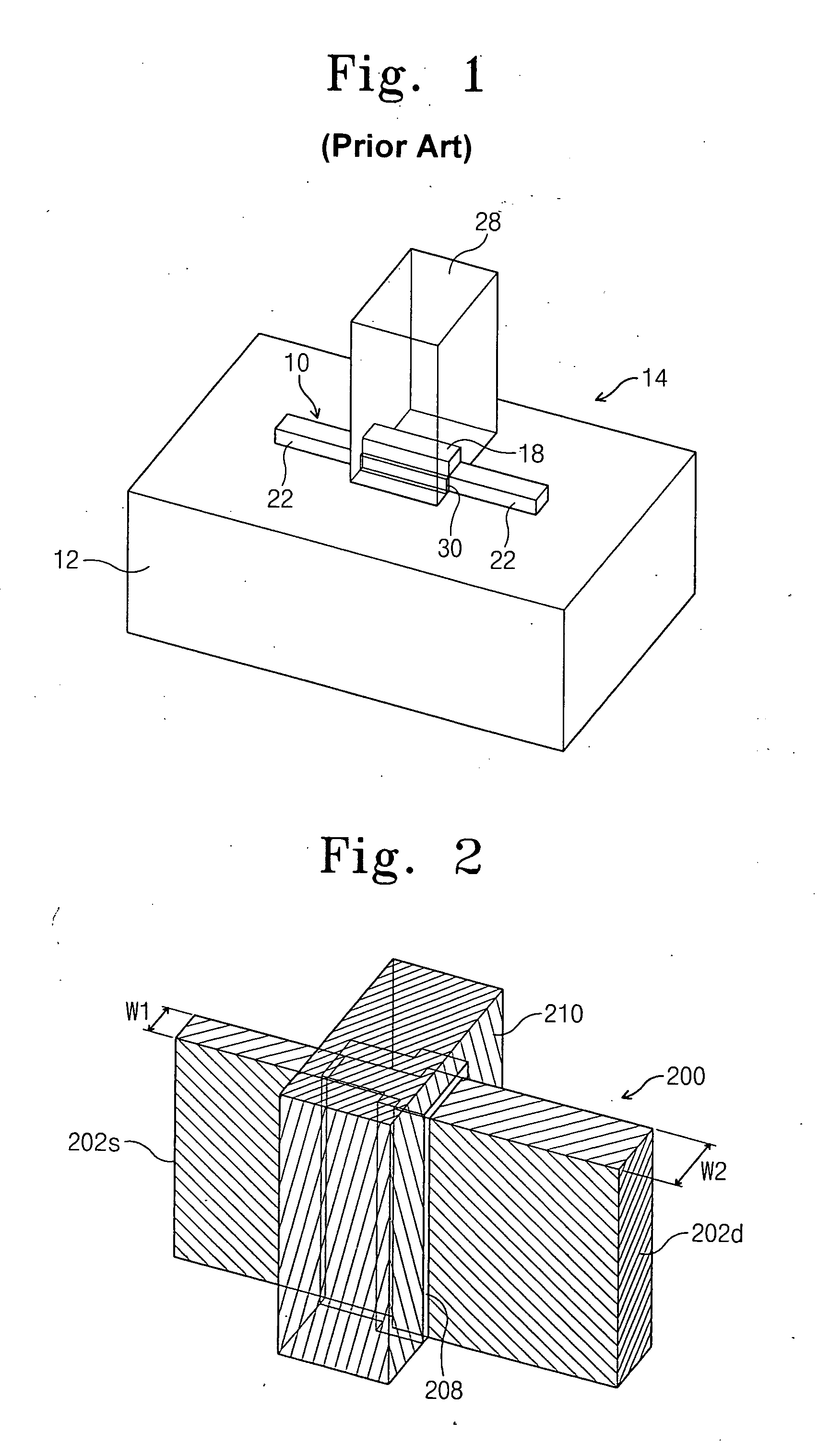
[0045]FIG. 2 is a perspective view of a FinFET in accordance with the present invention. The FinFET includes a fin 200 that is on a substrate, such as the substrate 12 of FIG. 1, and that extends laterally along the substrate and vertically away from the substrate. Accordingly, fin 200 may be referred to as vertically extending fin 200. The fin 200 includes a first region having a first fin width W1 and a second region having a second fin width W2 that is larger than the first fin width W1. A gate electrode 210 covers sides and a top of a portion of the fin 200. A gate insulation layer 208 is between the gate electrode 210 and the fin 200. A source region 202s and a drain regions 202d are formed in the fin 200 adjacent to opposite sides of the gate electrode 210. The source region 202s is formed in the first region of the fin 200, and the drain region 202d is formed in the second region 202s of the fin 200.

[0046] The gate electrode 210 covers a portion of the fin 200 that includes a...

second embodiment

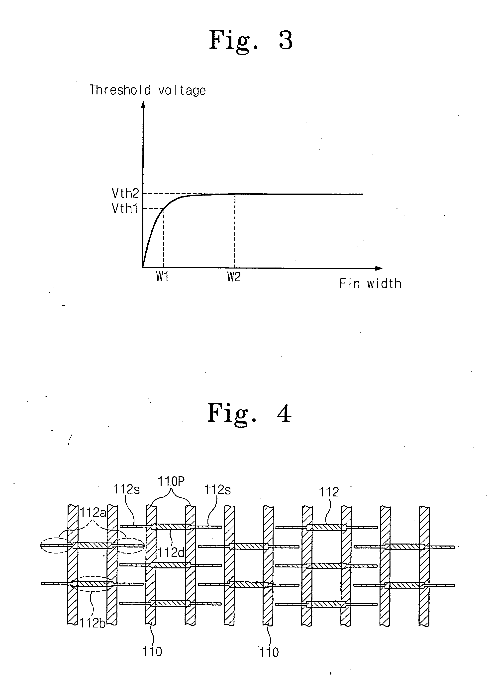
[0074] As previously explained, the FinFET according to the present invention may have a high threshold voltage while being turned off, so that the off leakage is low. The FinFET may also have a low threshold voltage while being turned on, so that a transistor on current is low. Because a doping concentration of the channel region that is adjacent to the source region is low, a junction leakage between a source region and a channel may be suppressed.

[0075] As shown in FIG. 11, the boundary region of the first region and the second region is covered by the gate electrode 210. In accordance with some embodiments of the present invention, the FinFET may include a fin that tapers off from a drain region 302d to a source region 302s (see FIG. 14A), or it may have a fin that has a larger width as it extends toward the drain region 312d than as it extends toward the source region 212s (e.g., FIG. 14B).

[0076]FIG. 15 is a perspective view of an alternate embodiment of the FinFET of FIG. 11 ...


PUM


Abstract

A fin field effect transistor (FinFET) includes a substrate, a fin, a gate electrode, a gate insulation layer, and source and drain regions in the fin. The fin is on and extends laterally along and vertically away from the substrate. The gate electrode covers sides and a top of a portion of the fin. The gate insulation layer is between the gate electrode and the fin. The source region and the drain region in the fin and adjacent to opposite sides of the gate electrode. The source region of the fin has a different width than the drain region of the fin.

Description

RELATED APPLICATION [0001] This application claims the benefit of and priority to Korean Patent Application No. 10-2004-0019711, filed Mar. 23, 2004, and to Korean Patent Application No. 10-2004-0071798, filed Sep. 8, 2004, the disclosures of which are hereby incorporated herein by reference. FIELD OF THE INVENTION [0002] The present invention relates to semiconductor devices, and, more particularly, a fin field effect transistor with a vertical channel and related methods of fabricating fin field effect transistors. BACKGROUND OF THE INVENTION [0003] The continuing trend to fabricate semiconductor devices with smaller device features has led to some difficulties when trying to scale-down transistors that have a horizontal channel (hereinafter referred to as “horizontal channel transistors”). Two difficulties that can arise when trying to scale-down horizontal channel transistors are short channel effect and drain induced barrier lower (DIBL) effect. When a channel length of a trans...

Claims


Application Information

Patent Timeline
Patent Type & Authority Applications(United States)
IPC IPC(8): H01L21/00H01L21/20H01L21/265H01L21/336H01L21/84H01L29/76H01L29/786H01L29/94H01L31/062H01L31/113H01L31/119
CPCH01L21/26513H01L21/845H01L29/78624H01L29/785H01L29/66795
Inventor LEE, CHULKIM, MIN-SANGPARK, DONG-GUNLEE, CHOONG-HOOH, CHANG-WOOYOON, JAE-MANKIM, DONG-WONCHOE, JEONG-DONGLI, MINGCHO, HYE-JIN
Owner SAMSUNG ELECTRONICS CO LTD
Learn More