Apparatus and method for manufacturing positive or negative microlenses

a microlens and array technology, applied in the field of microlens array structure and manufacturing methods, can solve the problems of increasing the crosstalk between adjacent pixels, increasing the difficulty of providing a microlens capable of focusing incident light rays onto the photosensitive regions, and small charge accumulation area in individual pixels in the array, so as to achieve the effect of small radius

Active Publication Date: 2005-12-08
MICRON TECH INC
View PDF16 Cites 37 Cited by
  • Summary
  • Abstract
  • Description
  • Claims
  • Application Information

AI Technical Summary

Benefits of technology

[0007] The various exemplary embodiments of the invention provide a variety of structures and methods used to adjust the shape, radius and / or height of a microlens for a pixel array. The embodiments use structures that affect volume and surface force parameters during microlens formation. Exemplary embodiments are directed to a microlens structure that includes a microlens frame, base, material, protrusions or a combination thereof to affect the shape, height and / or radius of the microlens. The frame, base and / or protrusions alter the microlens flow resulting from the heating of the microlens during fabrication such that a height or radius of the microlens can be controlled. The radius can be adjusted by the height differences between the microlens and frame. The bigger the difference, the smaller the radius will be.

Problems solved by technology

However, reductions in pixel sizes result in a smaller charge accumulation area in individual pixels in the array.
As the size of imager arrays and photosensitive regions of pixels decreases, it becomes increasingly difficult to provide a microlens capable of focusing incident light rays onto the photosensitive regions.
This problem is due in part to the increased difficulty in constructing a smaller microlens that has the optimal focal characteristics for the imager device process and that optimally adjusts for optical aberrations introduced as the light passes through the various device layers.
Also, it is difficult to correct possible distortions created by multiple regions above the photosensitive area, which results in increased crosstalk between adjacent pixels.
Microlens shaping and fabrication through heating and melting microlens materials also becomes increasingly difficult as microlens structures decrease in size.
Previous approaches to control microlens shaping and fabrication do not provide sufficient control to ensure optical properties such as focal characteristics, radius of a microlens or other parameters needed to provide a desired focal effect for smaller microlens designs.
Consequently, imagers with smaller sized microlenses have difficulty in achieving high color fidelity and signal / noise ratios.

Method used


Image

  • Apparatus and method for manufacturing positive or negative microlenses
  • Apparatus and method for manufacturing positive or negative microlenses
  • Apparatus and method for manufacturing positive or negative microlenses

Examples


Embodiment Construction

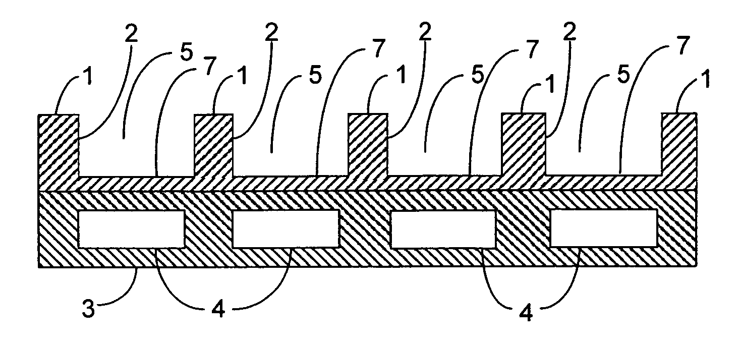
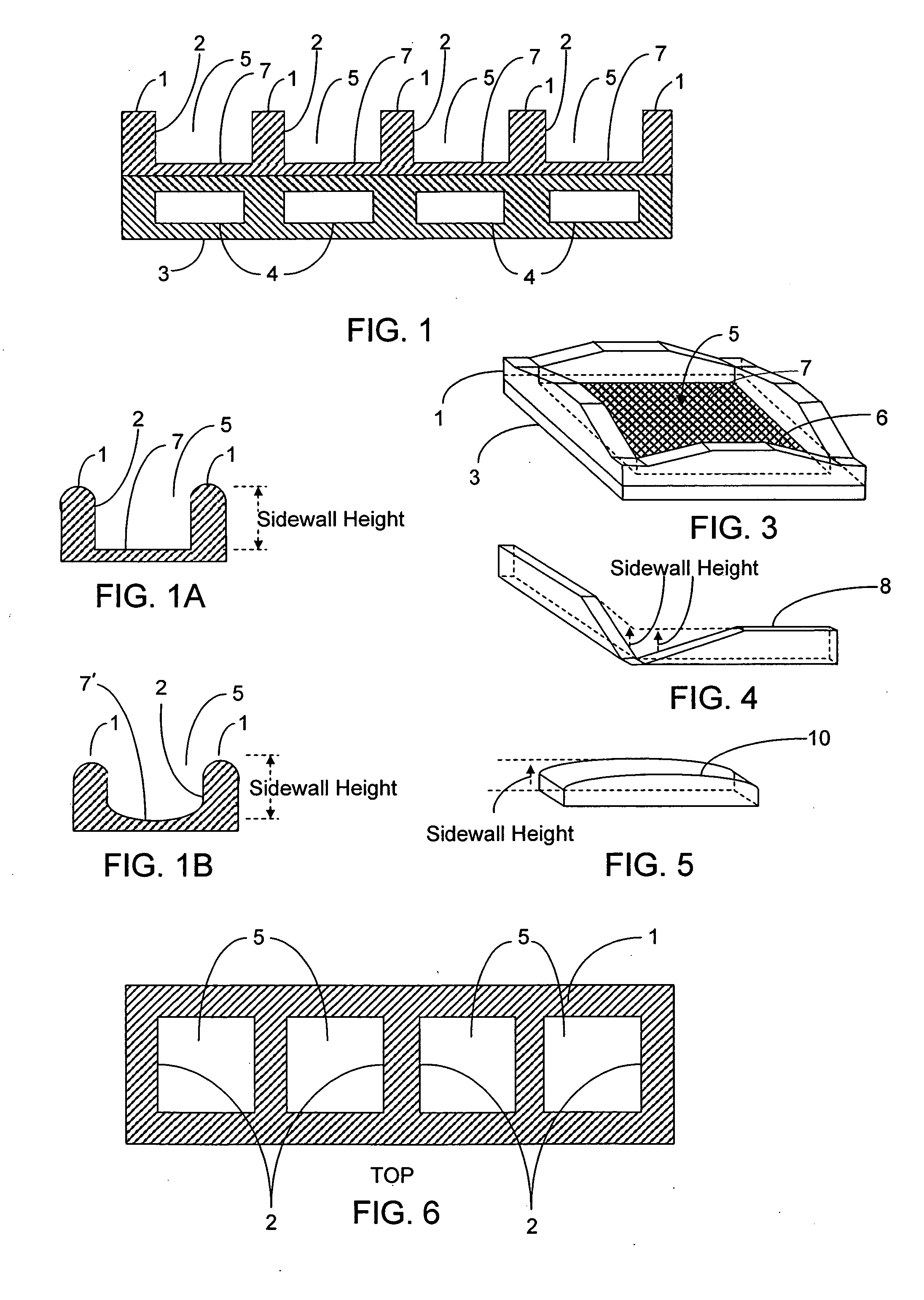
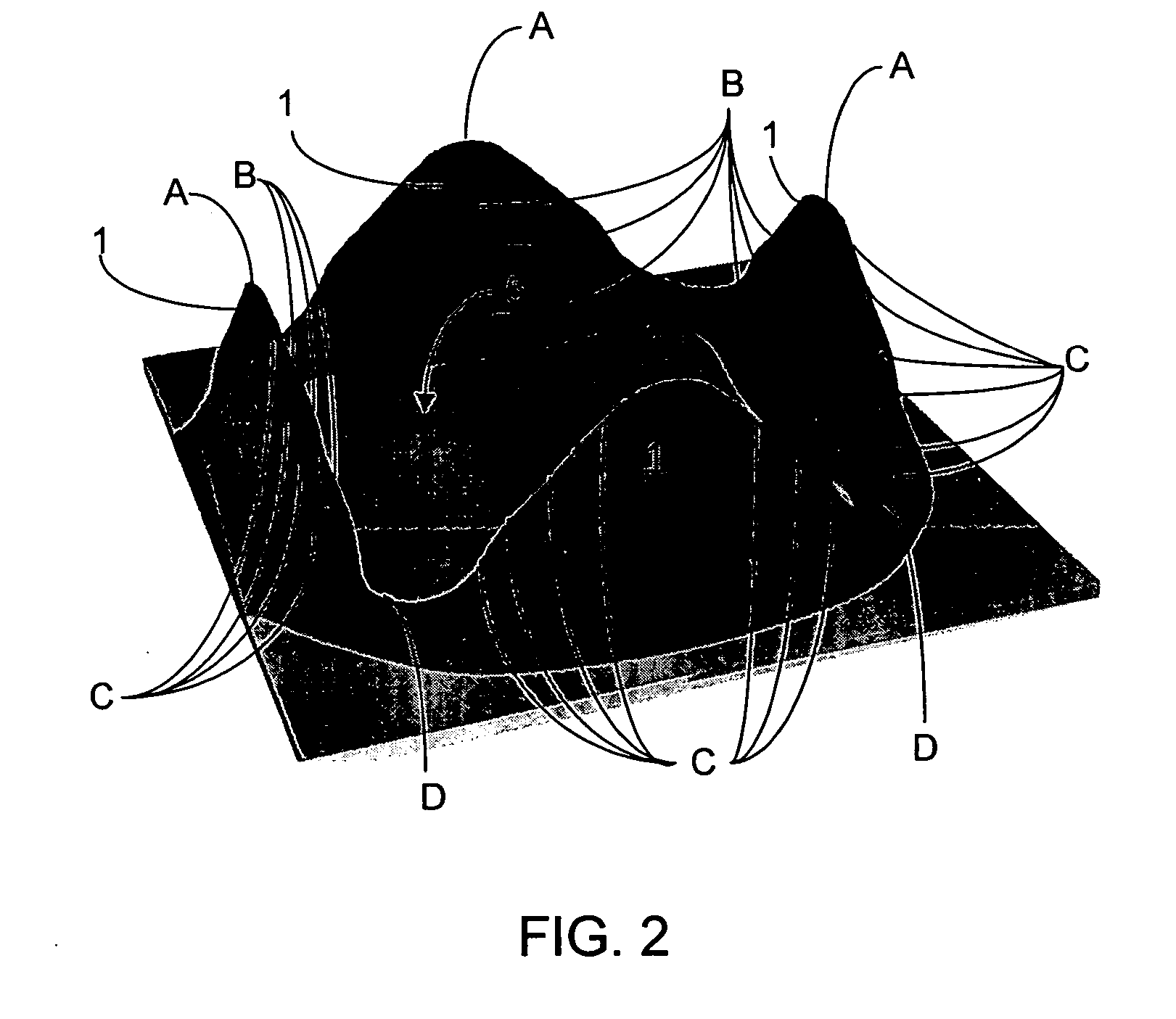
[0039] Exemplary embodiments of the invention affect or adjust microlens shapes or optical properties during lens formation (e.g., heating of lens material thereby causing lens material to flow or settle into an intended microlens shape). Microlens frames and / or other structures are used to affect or alter the flow behavior of lens material to be different than otherwise would occur without use of a microlens frame or other flow behavior altering structures.

[0040] According to the invention, the focal characteristics of a microlens can be adjusted by, among other things, forming boundary walls around lens materials to contain / limit the outward flow of lens material. This adjusts microlens flow behavior, e.g., increasing microlens height or defining a perimeter of the microlens structures. Boundary walls can be formed by formation of cavities or frame sidewalls with microlens material deposited therein. Post-flow microlens shapes can also be adjusted or affected by use of structures...


PUM

PropertyMeasurementUnit
temperatureaaaaaaaaaa
thicknessaaaaaaaaaa
thicknessaaaaaaaaaa

Abstract

A variety of structures and methods used to adjust the shape, radius and/or height of a microlens for a pixel array. The structures affect volume and surface force parameters during microlens formation. Exemplary microlens structures include a microlens frame, base, material, protrusions or a combination thereof to affect the shape, height and/or radius of the microlens. The frame, base and/or protrusions alter the microlens flow resulting from the heating of the microlens during fabrication such that a height or radius of the microlens can be controlled. The radius can be adjusted by the height differences between the microlens and frame. The bigger the difference, the smaller the radius will be.

Description

FIELD OF THE INVENTION [0001] The invention relates to fabrication of microlens structures for image capture or display systems, and more specifically to structures and methods of manufacturing of microlens arrays for solid state imager systems. BACKGROUND OF THE INVENTION [0002] Solid state imagers, including charge coupled devices (CCD) and CMOS sensors, have been commonly used in photo imaging applications. A solid state imager circuit includes a focal plane array of pixel cells, each one of the cells including either a photogate, photoconductor or a photodiode having a doped region for accumulating photo-generated charge. Microlenses are commonly placed over imager pixel cells. A microlens is used to focus light onto the initial charge accumulation region. Conventional technology uses a single microlens with a polymer coating, which is patterned into squares or circles provided respectively over the pixels which are then heated during manufacturing to shape and cure the microlen...

Claims


Application Information

Patent Timeline
Patent Type & Authority Applications(United States)
IPC IPC(8): B29D11/00G02B3/00G02B27/10G02F1/1335H01L27/146
CPCB29D11/00278B29D11/00365G02B3/0018G02B3/0056H01L27/14627H01L27/14685G02B27/10
Inventor BOETTIGER, ULRICH C.LI, JIN
Owner MICRON TECH INC
Why Eureka
Try Eureka