

Method for dicing substrate
a substrate and dicing technology, applied in the direction of manufacturing tools, semiconductor/solid-state device details, welding/soldering/cutting articles, etc., can solve the problems of side face chipping and cracking, and achieve the effect of preventing chipping and cracking and improving the transverse rupture strength of chips
- Summary
- Abstract
- Description
- Claims
- Application Information
AI Technical Summary
Benefits of technology
Problems solved by technology
Method used
Image

Examples
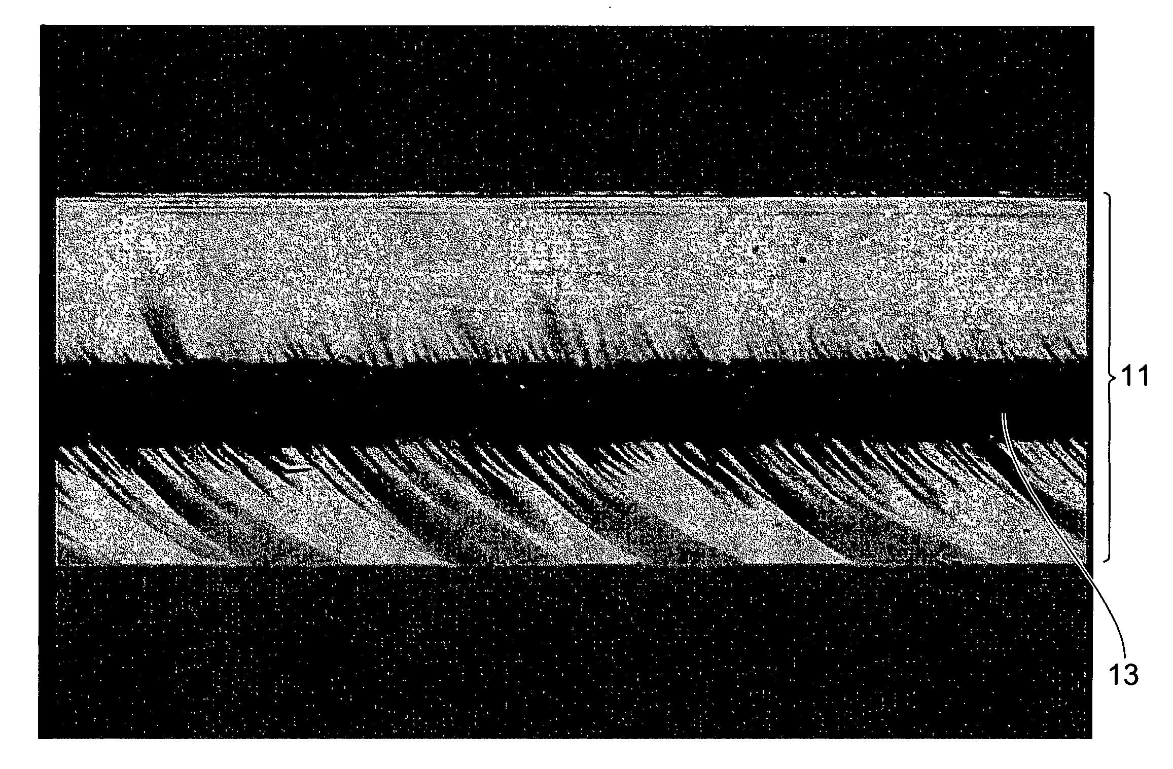
example 1
[0111] Example 1 of the substrate dividing method in accordance with the present invention will now be explained. Example 1 is directed to a case where the substrate 1 is a silicon wafer (having a thickness of 350 μm and an outer diameter of 4 inches) (“substrate 1” will hereinafter be referred to as “semiconductor substrate 1” in Example 1), whereas the front face 3 of the semiconductor substrate 1 is formed with a plurality of functional devices in a device manufacturing process.
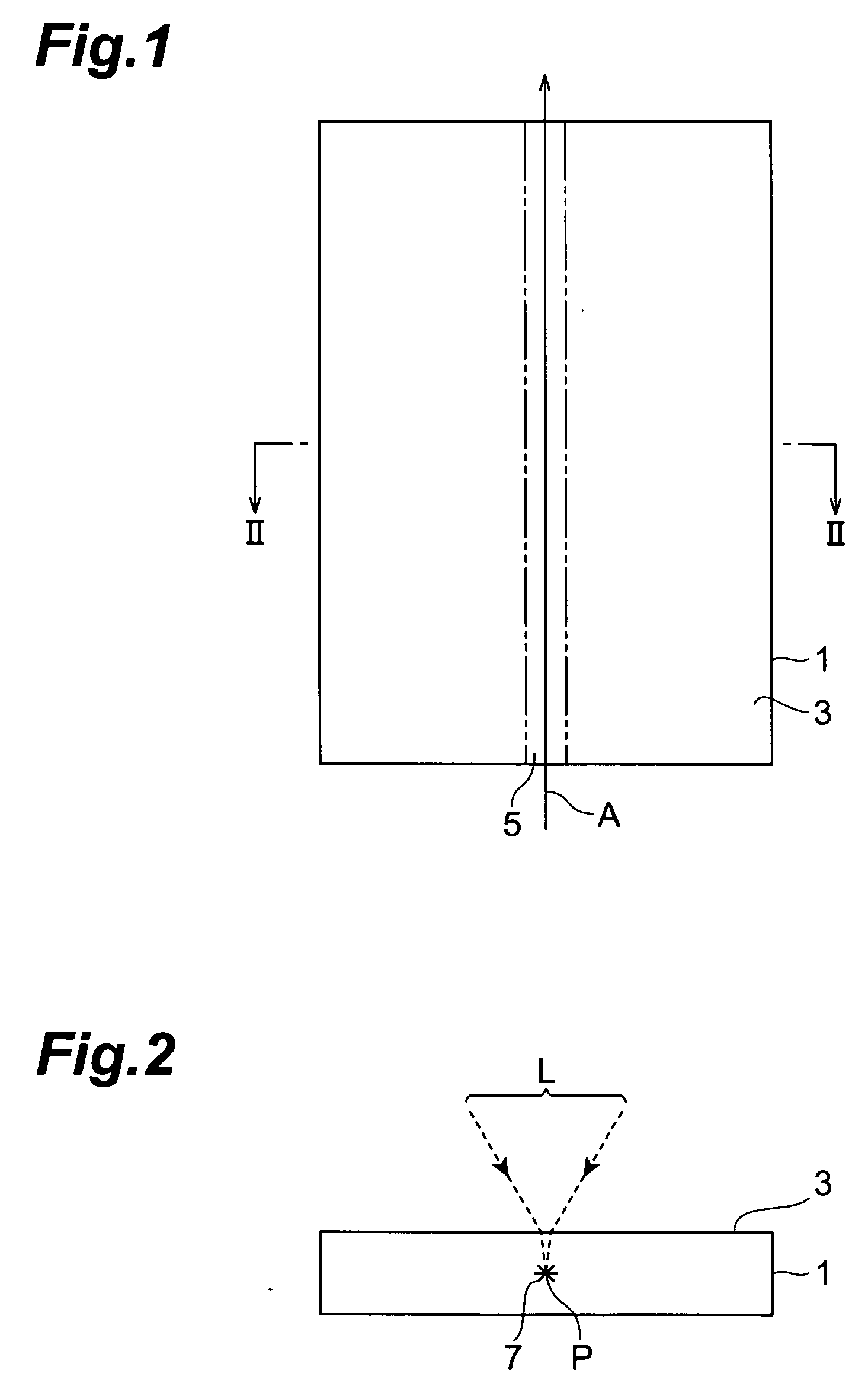
[0112] First, before explaining a step of forming a starting point region for cutting within the semiconductor substrate 1, a laser processing apparatus employed in the step of forming a starting point region for cutting will be explained with reference to FIG. 14. FIG. 14 is a schematic diagram of the laser processing apparatus 100.
[0113] The laser processing apparatus 100 comprises a laser light source 101 for generating laser light L; a laser light source controller 102 for controlling the laser light...
example 2
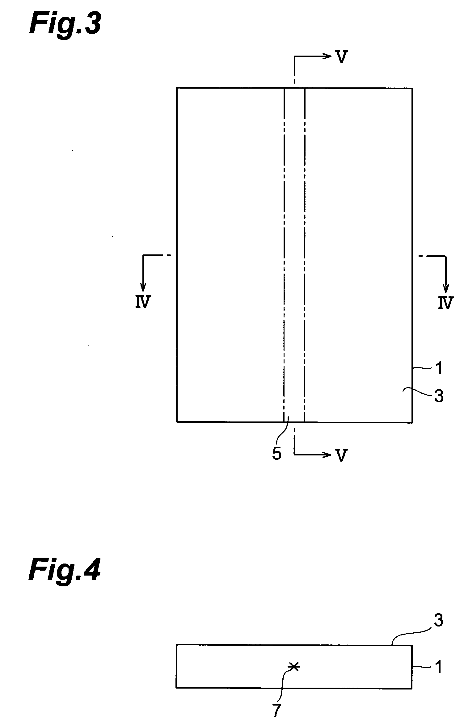
[0146] Example 2 of the substrate dividing method in accordance with the present invention will now be explained with reference to FIGS. 27 to 35. Example 2 relates to a case where the substrate 1 is a sapphire substrate (having a thickness of 450 μm and an outer diameter of 2 inches) which is an insulating substrate (“substrate 1” will hereinafter be referred to as “sapphire substrate 1” in Example 2), so as to yield a semiconductor chip to become a light-emitting diode. FIGS. 28 to 35 are sectional views of the sapphire substrate 1 taken along the line XX-XX of FIG. 27.
[0147] First, as shown in FIG. 28, the sapphire substrate 1 is irradiated with laser light L while a light-converging point P is positioned therewithin, so as to form a modified region 7 within the sapphire substrate 1. In a later step, a plurality of functional devices 19 are formed like a matrix on the front face 3 of the sapphire substrate 1, and the sapphire substrate 1 is divided into the functional devices 19...
PUM
| Property | Measurement | Unit |
|---|---|---|
| Time | aaaaa | aaaaa |
| Time | aaaaa | aaaaa |
| Thickness | aaaaa | aaaaa |
Abstract
Description
Claims
Application Information