Piezo resistance type semiconductor device and its manufacturing method

a semiconductor device and resistance technology, applied in the direction of acceleration measurement using interia force, acceleration measurement in multiple dimensions, instruments, etc., can solve the problems of increasing the manufacturing cost of the semiconductor device, the diaphragm is broken in this portion, and the sensitivity of stress detection precision is deteriorating, so as to improve the linearity of output and the sensitivity of detection. , the effect of mechanical strength reduction

Inactive Publication Date: 2005-12-15
CANON KK
View PDF1 Cites 35 Cited by
  • Summary
  • Abstract
  • Description
  • Claims
  • Application Information

AI Technical Summary

Benefits of technology

[0018] By constructing the semiconductor device as mentioned above, the stresses can be concentrated on the piezo resistance type stress detector 4 without causing the mechanical strength to be remarkably decreased in the diaphragm portion. The electric insulati...

Problems solved by technology

There is a fear that when the excessive external force is applied, the diaphragm is broken in this portion.
The piezo resistance type stress detector has a high resistance and the...

Method used


Image

  • Piezo resistance type semiconductor device and its manufacturing method
  • Piezo resistance type semiconductor device and its manufacturing method
  • Piezo resistance type semiconductor device and its manufacturing method

Examples


first embodiment

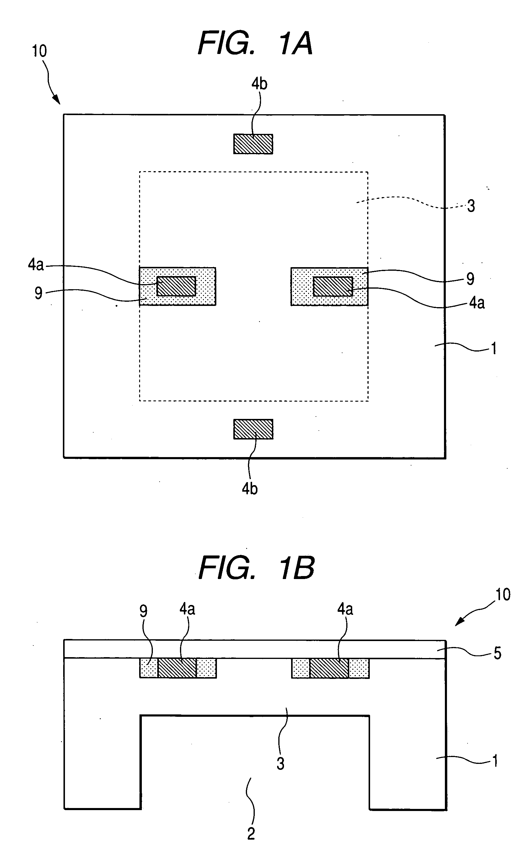
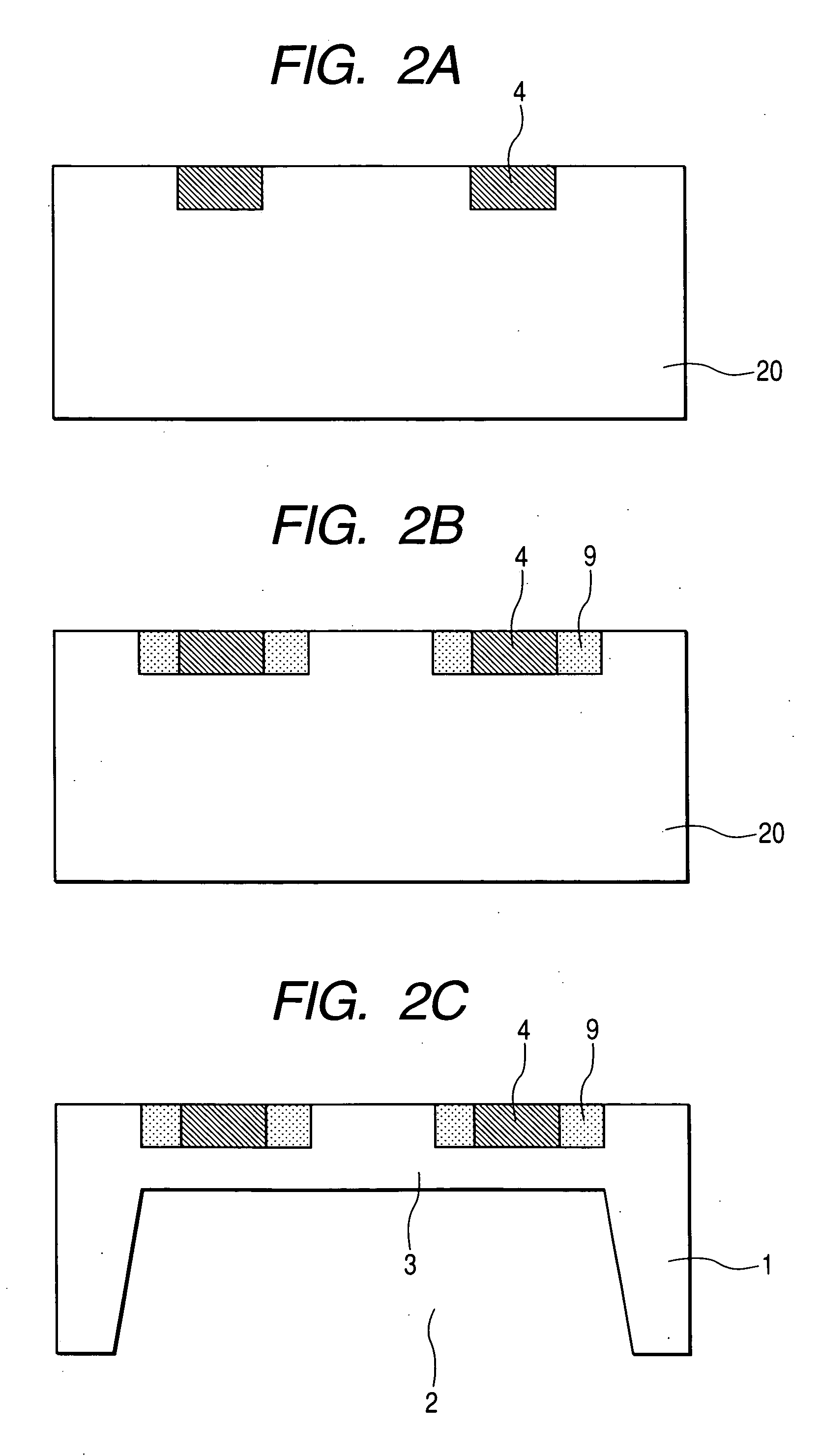
[0038]FIGS. 1A and 1B are a plan view and a cross sectional view of a piezo resistance type pressure sensor as a kind of piezo resistance type semiconductor device according to the first embodiment of the invention.

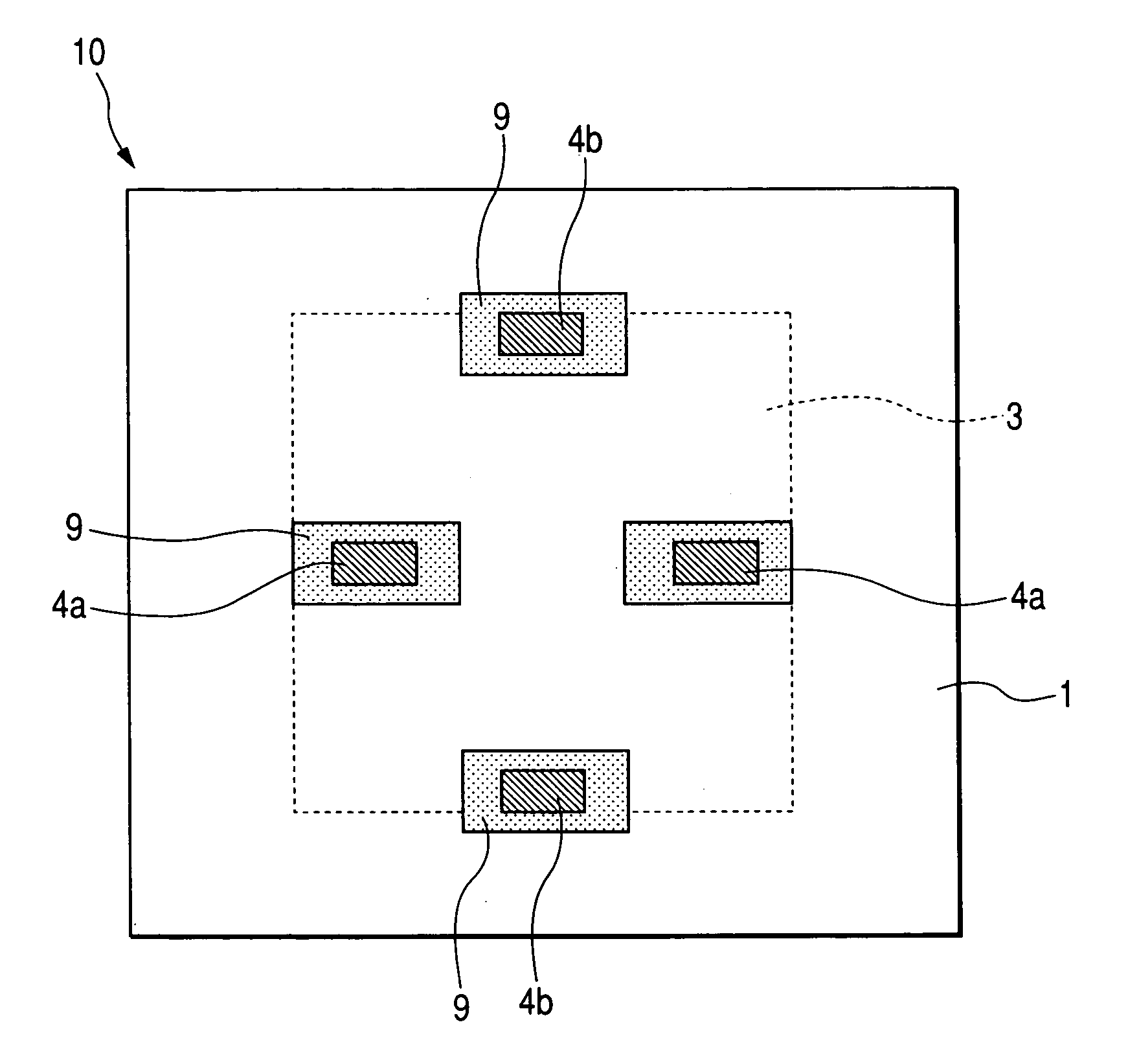
[0039] The piezo resistance type pressure sensor 10 shown in the diagrams uses a semiconductor substrate made of, for example, silicon and the hollow portion 2 is formed from the back surface side of the semiconductor substrate. The semiconductor substrate of the upper surface portion of the hollow portion 2 is used as a diaphragm 3. The diaphragm 3 has a rectangular or square flat shape. Since the portion (external periphery) surrounding the diaphragm 3 is not the hollow portion 2, a thickness of semiconductor substrate in this portion is larger than that of the region of the diaphragm 3 in correspondence to the portion of the absence of the hollow portion 2 and such an external periphery is constructed as a supporting frame 1 for the diaphragm 3.

[0040] Stress detector...

second embodiment

[0048] The second embodiment of the invention will now be described. FIGS. 3A and 3B are a plan view and a cross sectional view of a piezo resistance type pressure sensor as a kind of piezo resistance type semiconductor device according to the second embodiment of the invention.

[0049] Although the piezo resistance type pressure sensor of the second embodiment is similar to that of the first embodiment, the sensor of the second embodiment differs from that of the first embodiment with respect to a point that the diaphragm 3 is formed so as to have an SOI structure by using what is called an SOI (Semiconductor On Insulator) substrate as a semiconductor substrate, and the stress detectors 4b are also formed on the diaphragm 3 and the groove 9 is also formed in the periphery of each stress detector 4b. Specifically speaking, a buried insulation layer 11 and a monocrystalline semiconductor layer 12 are laminated on a silicon semiconductor layer (bulk layer) of a thick bulk in this order...

third embodiment

[0054] The third embodiment of the invention will now be described. FIGS. 5A and 5B are a plan view and a cross sectional view of a piezo resistance type pressure sensor as a kind of piezo resistance type semiconductor device according to the third embodiment of the invention.

[0055] The piezo resistance type pressure sensor of the third embodiment differs from that of the second embodiment with respect to a point that in at least one of the piezo resistance type stress detectors 4a and 4b, the groove 9 around the stress detector reaches a buried insulation layer 11. The groove 9 which reaches the buried insulation layer 11 completely surrounds the corresponding stress detector. By constructing the device as mentioned above, the PN junction leakage between the stress detectors and that between the stress detector and the monocrystalline semiconductor layer 12 can be suppressed. Along with the stress concentration on the stress detectors, the detecting sensitivity of the pressure sen...


PUM


Abstract

In a piezo resistance type semiconductor device, a detecting sensitivity and output linearity are improved without increasing a forming region of a diaphragm. In a piezo resistance type semiconductor device having: a diaphragm; a supporting frame which is connected to an external periphery of the diaphragm, supports the diaphragm, and is formed relatively thicker than the diaphragm; and piezo resistance type stress detectors (4a, 4b) each for detecting a stress caused when the detector is distorted by deformation of the diaphragm by application of an acceleration or a pressure in the direction perpendicular to the diaphragm, at least a part of the diaphragm is cut off in a position where it is come into contact with the piezo resistance type stress detector and a groove is formed.

Description

BACKGROUND OF THE INVENTION [0001] 1. Field of the Invention [0002] The invention relates to a piezo resistance type semiconductor device formed by arranging a piezo resistor onto a semiconductor substrate and, more particularly, to a piezo resistance type semiconductor device in which detecting sensitivity is improved without increasing an area of a forming region of a diaphragm on a semiconductor substrate. [0003] 2. Related Background Art [0004] In recent years, sensors to detect various physical amounts have been manufactured by applying a semiconductor device manufacturing technique. Semiconductor devices such as pressure sensor, acceleration sensor, and the like have also been manufactured as piezo resistance type semiconductor devices on the basis of the semiconductor device manufacturing technique. The piezo resistance type semiconductor devices are widely used in the fields of automobiles, household appliances, industrial apparatuses, measuring instruments, medical equipmen...

Claims


Application Information

Patent Timeline
IPC IPC(8): G01L9/00G01L9/06G01P15/08G01P15/12H01L29/84
CPCG01L9/0055G01P15/0802G01P15/123G01P15/18G01P2015/084
Inventor HASEGAWA, SHINKOKUMAI, KAZUO
Owner CANON KK
Why Eureka
Try Eureka