Organic bistable memory and method of manufacturing the same

a memory and organic technology, applied in thermoelectric devices, instruments, nanoinformatics, etc., can solve the problems of increasing the on/off current ratio of the memory, prolonging the retention time, and difficult control of the organic bistable memory

Inactive Publication Date: 2005-12-15
IND TECH RES INST
View PDF6 Cites 24 Cited by
  • Summary
  • Abstract
  • Description
  • Claims
  • Application Information

AI Technical Summary

Benefits of technology

[0025]FIG. 7 is the organic bistable memory according to the invention where the dielectri...

Problems solved by technology

Patent # WO0237500 has disclosed organic bistable memory that has the disadvantage of being difficult to control because of varying quality of the organic material used and conditions of manufacturing the memory device.
Organic materials of good quality used for the memory may increase the on/off current ratio of the memory and prolong retention time, while organic materials of inferior qualit...

Method used


Image

  • Organic bistable memory and method of manufacturing the same
  • Organic bistable memory and method of manufacturing the same
  • Organic bistable memory and method of manufacturing the same

Examples


second embodiment

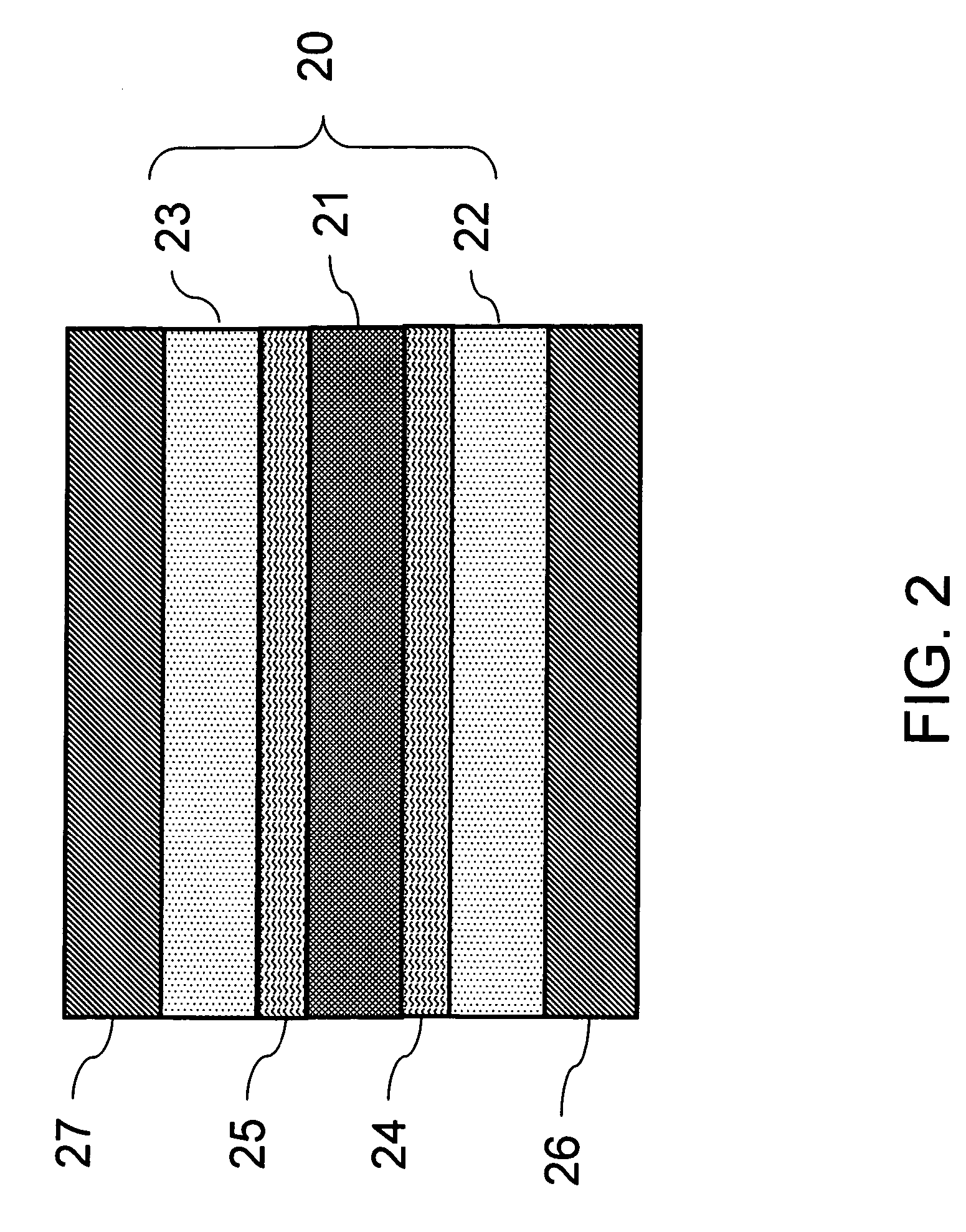
[0029] Reference is made to FIG. 2, which is a structural schematic of the organic bistable memory according to the invention. The embodiment comprises a bistable body 20 with a conductive layer 21, a first organic layer 22 and a second organic layer 23. On two sides of the conductive layer 21, a first dielectric layer 24 and a second dielectric layer 25 are respectively formed. The side of the first organic layer 22 not in contact with the bistable body 20 is formed with a first electrode 26, and the side of the second organic layer 23 not in contact with the bistable body 20 is formed with a second electrode 27.

third embodiment

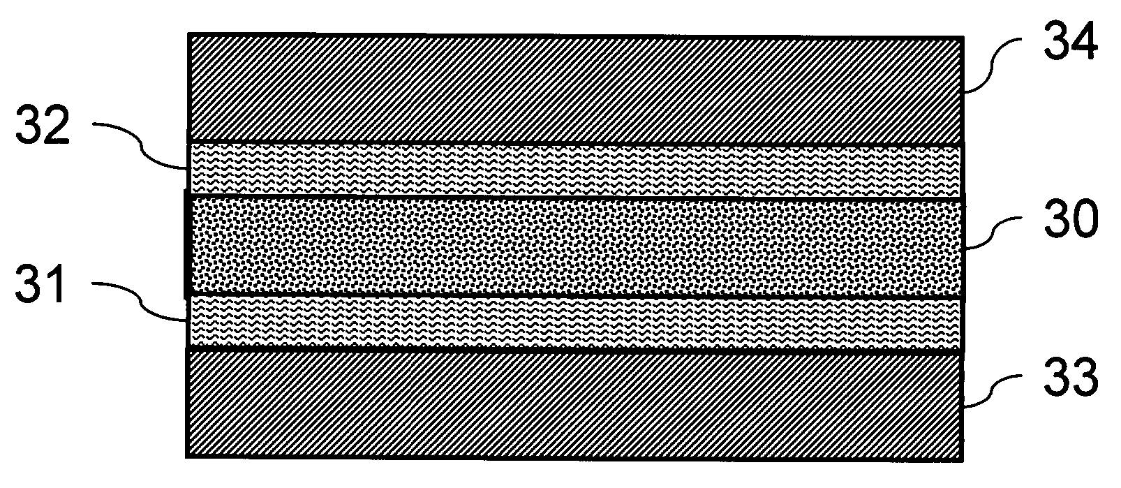
[0030] Refer to FIG. 3, which is a structural schematic of the organic bistable memory according to the invention. This embodiment comprises a bistable body 30 composed of a material with nanoparticles of high conduction and a material of low conduction. On two sides of the bistable body 30, a first dielectric layer 31 and a second dielectric layer 32 are formed. The side of the first dielectric layer 31 not in contact with the bistable body 30 is formed with a first electrode 33, and the side of the second dielectric layer 32 not in contact with the bistable body 30 is formed with a second electrode 34.

[0031] According to the invention, the conductive layers and the organic layers in the first, second, and third embodiments are the same. The conductive layer may be a material of high conduction, such as metal and super-conductive material, which may be aluminum, copper or silver. Other materials with high work function such as gold and nickel, materials with middle work function su...


PUM

PropertyMeasurementUnit
Timeaaaaaaaaaa
Thicknessaaaaaaaaaa
Thicknessaaaaaaaaaa

Abstract

An organic bistable memory device has an organic layer with two sides, each having a dielectric layer with an electrode. When voltage is applied to the two electrodes, the memory may be switched and operated between a high impedance state and a low impedance state. This reduces negative effects on the memory device due to poor quality material or non-uniform manufacturing of the device, effects such as reduced on/off current ratio, shortened retention time and shorting failure in the device. Also, the disclosed organic bistable memory provides evidence to improve our understanding of bistable memory.

Description

[0001] This Non-provisional application claims priority under 35 U.S.C. § 119(a) on Patent Application No(s). 093116692 filed in Taiwan on Jun. 10, 2004, the entire contents of which are hereby incorporated by reference. BACKGROUND OF THE INVENTION [0002] 1. Field of Invention [0003] The invention relates to a memory device, and particularly to an organic bistable memory device. [0004] 2. Related Art [0005] Memory is indispensable to a modem computer. Integration degree of dynamic random access memory (DRAM) may be an important index to semiconductor technology. Organic materials have recently been introduced and used in memory in order to achieve higher integration and power saving purposes. [0006] Among organic memory devices, the organic bistable device (OBD) is a promising memory device. Patent # WO0237500 has disclosed organic bistable memory that has the disadvantage of being difficult to control because of varying quality of the organic material used and conditions of manufac...

Claims


Application Information

Patent Timeline
IPC IPC(8): G11C13/02G11C11/36H01L27/10
CPCB82Y10/00G11C13/0014G11C13/0016G11C2213/15G11C2213/55H01L27/285H01L51/0035H01L51/0051H01L51/0081H10K19/202H10K85/111H10K85/611H10K85/324
Inventor CHEN, WEI-SU
Owner IND TECH RES INST
Why Eureka
Try Eureka