Fuse and write method for fuse

a fuse and write method technology, applied in the field of fuse, can solve the problems of large write current, and achieve the effects of preventing the increase of the whole chip area, reducing the write voltage and the write current, and preventing the increase of the cell area of the driving transistor

Inactive Publication Date: 2005-12-15
PANASONIC CORP
View PDF2 Cites 13 Cited by
  • Summary
  • Abstract
  • Description
  • Claims
  • Application Information

AI Technical Summary

Benefits of technology

[0051] Furthermore, since both the write voltage and the write current can be reduced, when the fuse of this invention is used in, for example, a PROM circuit, increase of a cell area of a driving transistor can be prevented, resulting in preventing the increase of the whole chip area.
[0052] In one aspect, the positive terminal side joint preferably has higher heat conductivity than the negative terminal side joint.
[0053] Herein, the heat conductivity means the heat conductivity of the whole positive terminal side joint and that of the whole negative terminal side joint.
[0054] In this manner, since the positive terminal side joint has higher heat conductivity and a larger heat radiation effect, the peak of the temperature distribution in the fusing part attained in fusing can be definitely prevented from shifting toward the positive terminal side joint. Accordingly, as described above, the positive terminal side joint can be prevented from being partly melted, resulting in preventing the increase of the write current.
[0055] In another aspect, the positive terminal side joint preferably has lower resistance than the negative terminal side joint.
[0056] In this manner, Joule heat generated in the positive terminal side joint is reduced, and therefore, the peak of the temperature distribution in the fusing part attained in fusing can be prevented from shifting toward the positive terminal side joint. Accordingly, as described above, the increase of the write current can be prevented. Also, since the negative terminal side joint has given resistance higher than the positive terminal side joint, as compared with the conventional technique in which the resistances of both the positive terminal side joint and the negative terminal side joint are reduced, an excessive current can be prevented from flowing when a filament is formed in fusing.

Problems solved by technology

In using the conventional polysilicon fuse, however, when the write voltage is lowered, the write current becomes large.

Method used


Image

  • Fuse and write method for fuse
  • Fuse and write method for fuse
  • Fuse and write method for fuse

Examples


embodiment 1

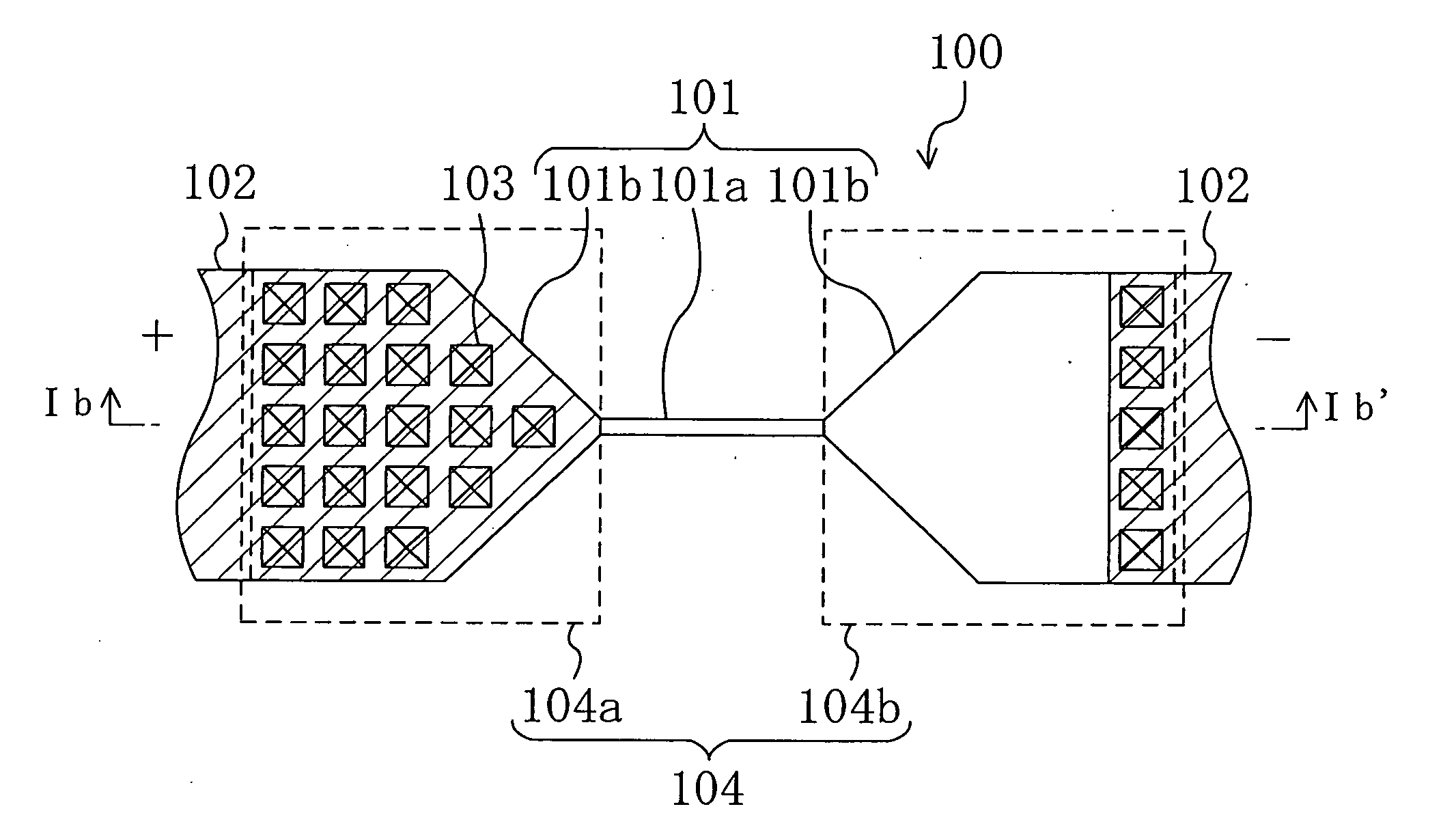
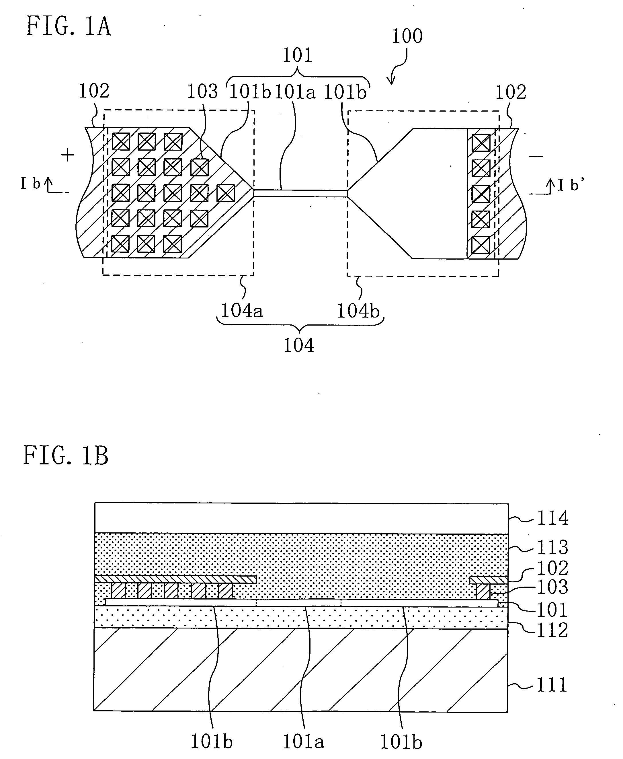
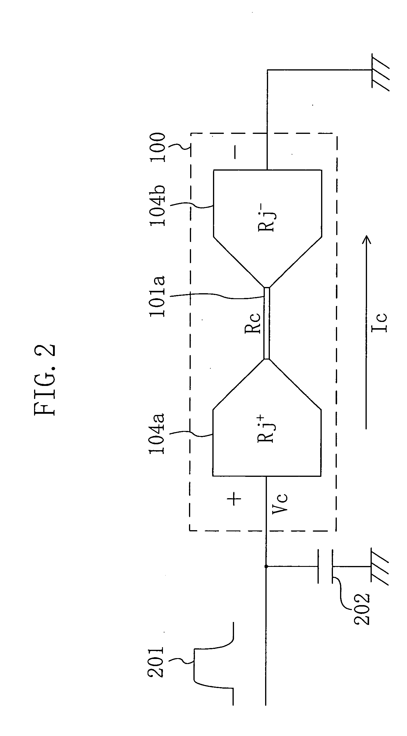
[0117]FIGS. 1A and 1B are diagrams of a semiconductor device including a polysilicon fuse according to Embodiment 1, and specifically, FIG. 1A is a plan view thereof where the polysilicon fuse 100 alone is perspectively shown and FIG. 1B is a cross-sectional view taken on line Ib-lb′ of FIG. 1A.

[0118] As shown in FIG. 1A, the polysilicon fuse 100 includes a fuse layer 101, an interconnect layer 102 and contacts 103 for electrically connecting the fuse layer 101 and the interconnect layer 102 to each other.

[0119] The fuse layer 101 is composed of a fusing part 101a to be fused through voltage application and a connecting part 101b connected to each end of the fusing part 101a, and at least a portion of each connecting part 101b disposed on the other side of the fusing part 101a is used as an interconnect region (not shown) to be connected to the interconnect layer 102.

[0120] Also, an interconnect (not shown) is connected to the polysilicon fuse 100 for voltage application or the l...

embodiment 2

[0146] A polysilicon fuse according to Embodiment 2 of the invention will now be described.

[0147]FIGS. 3A and 3B are diagrams of a semiconductor device including a polysilicon fuse according to Embodiment 2, and specifically, FIG. 3A is a plan view thereof where the polysilicon fuse 200 alone is perspectively shown and FIG. 3B is a cross-sectional view taken on line IIIb-IIIb′ of FIG. 3A.

[0148] In FIGS. 3A and 3B, like reference numerals are used to refer to like elements used in Embodiment 1 shown in FIGS. 1A and 1B and the detailed description is herein omitted.

[0149] The polysilicon fuse 200 of this embodiment is different from that of Embodiment 1 in the width of the negative terminal side joint 104b being smaller than that of the positive terminal side joint 104a, whereas the “width” herein means a width of the positive terminal side joint 104a or the negative terminal side joint 104b excluding its tapered portion in the vicinity of the fusing part 101a.

[0150] Since the res...

embodiment 3

[0154] A polysilicon fuse according to Embodiment 3 of the invention will now be described.

[0155]FIGS. 4A and 4B are diagrams of a semiconductor device including a polysilicon fuse according to Embodiment 3, and specifically, FIG. 4A is a plan view thereof where the polysilicon fuse 300 alone is perspectively shown and FIG. 4B is a cross-sectional view taken on line IVb-IVb′ of FIG. 4A.

[0156] In FIGS. 4A and 4B, like reference numerals are used to refer to like elements used in Embodiment 1 shown in FIGS. 1A and 1B and the detailed description is herein omitted.

[0157] The polysilicon fuse 300 of this embodiment is different from that of Embodiment 1 in the negative terminal side joint 104b being narrower than the positive terminal side joint 104a in the vicinity of the fusing part 101a. This will now be specifically described.

[0158] The positive terminal side joint 104a is in a taper shape that is linearly tapered toward the fusing part 101a from a position away by a given dista...


PUM


Abstract

A polysilicon fuse includes a fusing part to be fused through voltage application, a positive terminal side joint connected to one end of the fusing part and a negative terminal side joint connected to the other end of the fusing part. The positive terminal side joint that attains a high voltage through the voltage application has lower resistance and higher heat conductivity than the negative terminal side joint. Furthermore, a write operation is performed, with a current limiting resistance serially connected to a positive terminal side joint of a polysilicon fuse, by applying a voltage pulse to the polysilicon fuse through the current limiting resistance. Thus, a current flowing to the polysilicon fuse in fusing the fusing part is limited to a given range.

Description

CROSS-REFERENCE TO RELATED APLICATIONS [0001] This application claims priority under 35 U.S.C. §119 on Patent Application No. 2004-293444 filed in Japan on Oct. 6, 2004, the entire contents of which are hereby incorporated by reference. BACKGROUND OF THE INVENTION [0002] The present invention relates to a fuse, and more particularly, it relates to a fuse in which a write current and a write voltage are reduced and a write method for a fuse in which a write current can be reduced. [0003] A conventionally used fuse, such as a polysilicon fuse, includes a fusing part that is fused through voltage application; a positive terminal side joint that is connected to one end of the fusing part and to which a voltage is applied; and a negative terminal side joint connected to the other end of the fusing part. The positive terminal side joint and the negative terminal side joint have the same structure and the same property. [0004] In a polysilicon fuse, one of some kinds of structures is used ...

Claims


Application Information

Patent Timeline
Patent Type & Authority Applications(United States)
IPC IPC(8): H01L23/525G11C17/18H01L33/00H01L27/10H01L21/82
CPCG11C17/18H01L23/5256H01L2924/0002H01L2924/00
Inventor MATSUNAGA, TOMOHIRO
Owner PANASONIC CORP
Why Eureka
Try Eureka