Single metal gate material CMOS using strained si-silicon germanium heterojunction layered substrate

a technology of si-silicon germanium and heterojunction layered substrate, which is applied in the direction of basic electric elements, electrical apparatus, and semiconductor devices, can solve the problems of not teaching or suggesting the use of a single metal-gate material cmos using a strained si/sige heterojunction layered substrate, and the achievement of the appropriate workfunction of the n- and p-channel devices remains problematic, so as to improve the device operating speed, improve the transport properties of the carriers, and improve device speed

Inactive Publication Date: 2005-12-15
MASSACHUSETTS INST OF TECH
View PDF7 Cites 33 Cited by
  • Summary
  • Abstract
  • Description
  • Claims
  • Application Information

AI Technical Summary

Benefits of technology

[0016] Hence, the present invention allows utilization of a single metal material as the optimized metal-gate electrode for both n- and p-MOSFETs. The Ge content and thickness of the materials in the heterojunction substrate are adjusted to obtain the correct threshold voltage for both n- and p-MOSFETs, for a single metal-gate electrode materia

Problems solved by technology

In addition, none of the references achieve enhanced electron and hole mobilities simultaneous with the use of a single metal-gate material.
Jung et al. however, fail to teach or suggest the use of a single metal-gate material CMOS using a strained Si/SiGe heterojunction layered substrate.
(entitled “Dual Work Function Metal Gate

Method used


Image

  • Single metal gate material CMOS using strained si-silicon germanium heterojunction layered substrate
  • Single metal gate material CMOS using strained si-silicon germanium heterojunction layered substrate
  • Single metal gate material CMOS using strained si-silicon germanium heterojunction layered substrate

Examples


Embodiment Construction

[0023] While this invention is illustrated and described in a preferred embodiment, the invention may be produced in many different configurations. There is depicted in the drawings, and will herein be described in detail, a preferred embodiment of the invention, with the understanding that the present disclosure is to be considered as an exemplification of the principles of the invention and the associated functional specifications for its construction and is not intended to limit the invention to the embodiment illustrated. Those skilled in the art will envision many other possible variations within the scope of the present invention.

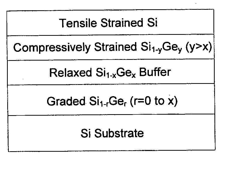
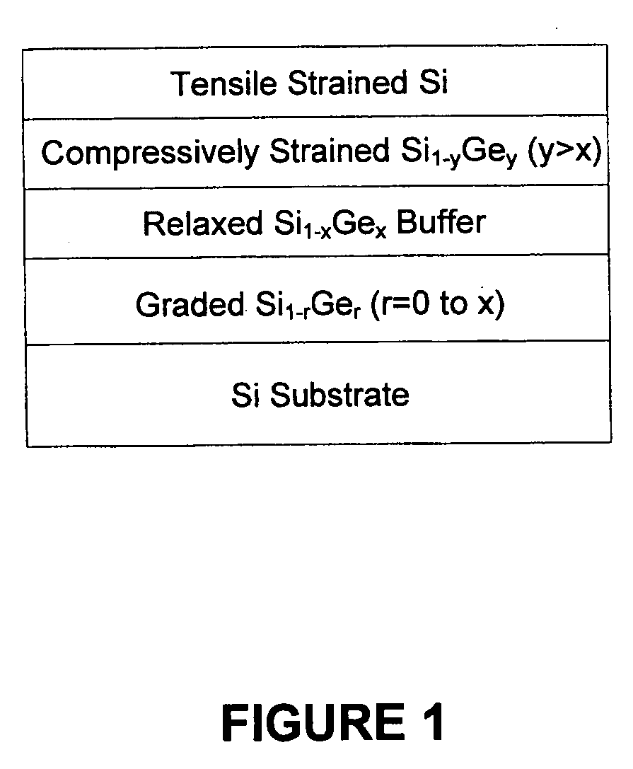
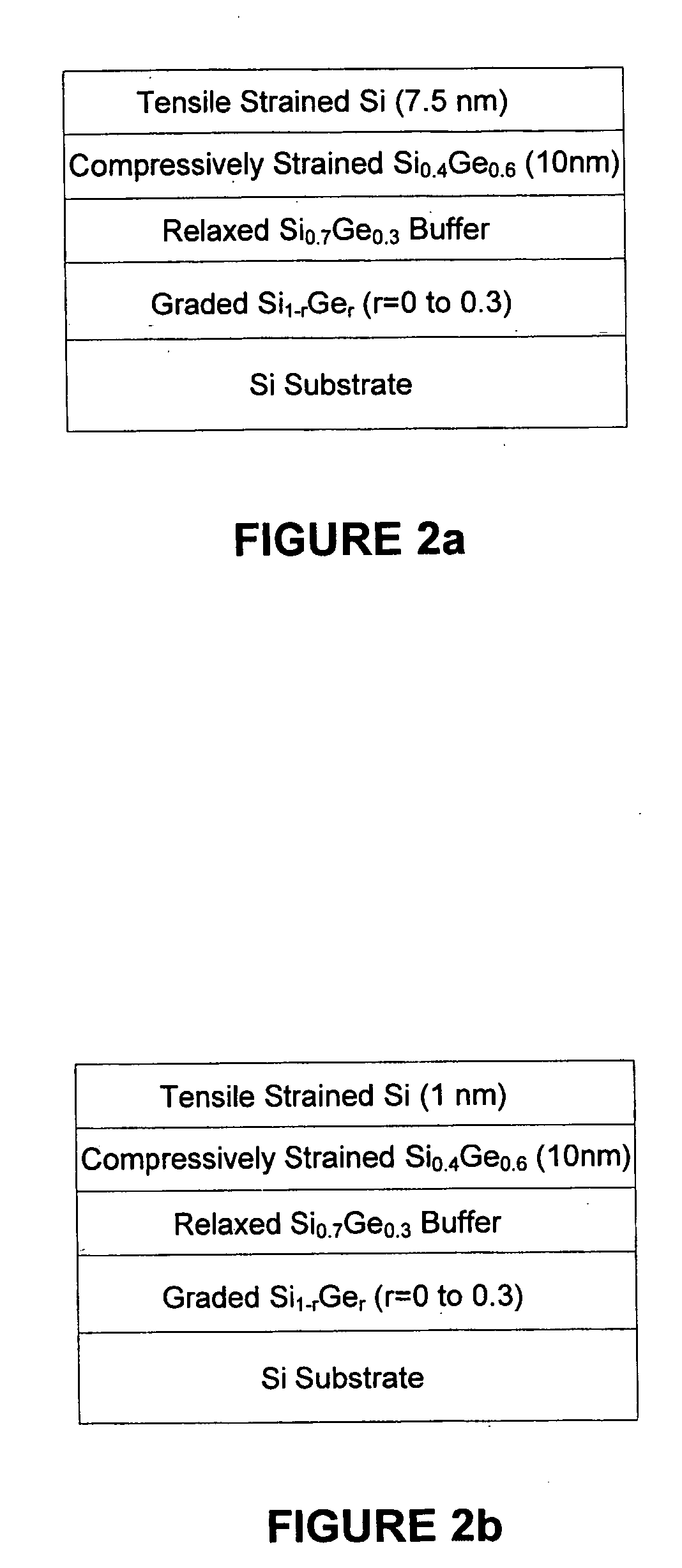
[0024] Metal-gate electrode has been regarded as one of the main technology enablers for continued scaling of Si based CMOS down to nanometer scale. Due to the nature of band energy structure of conventional Si substrate, the metal workfunction that is required to optimize n-channel MOSFET performance differs from that of p-channel MOSFET by a wide r...


PUM


Abstract

Strained Si/strained SiGe dual-channel layer substrate provides mobility advantage and when used as a CMOS substrate enables single workfunction metal-gate electrode technology. A single metal electrode with workfunction of 4.5 eV produces near ideal CMOS performance on a dual-channel layer substrate that consists sequentially of a silicon wafer, an epitaxially grown 30% Ge relaxed SiGe layer, a compressively strained 60% Ge layer, and a tensile-strained Si cap layer.

Description

PRIORITY INFORMATION [0001] This application claims priority to U.S. Provisional Patent Application Ser. No. 60 / 575,039, filed May 27, 2004, which is incorporated herein by reference in its entirety.BACKGROUND OF THE INVENTION [0002] 1. Field of Invention [0003] The present invention relates generally to the field of semiconductor substrates. More specifically, the present invention is related to the use of a single metal-gate material CMOS using strained Si / SiGe heterojunction layered substrate. [0004] 2. Discussion of Prior Art [0005] The references described below provide a general teaching in the area of substrate structures with enhanced electron and hole mobilities and in the area of integrating metal-gates, but none of the references teach or suggest the use of a single metal-gate material CMOS enabled by the use of a strained Si / SiGe heterojunction layered substrate. In addition, none of the references achieve enhanced electron and hole mobilities simultaneous with the use o...

Claims


Application Information

Patent Timeline
IPC IPC(8): H01L21/8238H01L29/10H01L29/49H01L29/78H01L31/0328
CPCH01L21/823807H01L21/823828H01L29/1054H01L29/4966H01L29/78
Inventor ANTONIADIS, DIMITRI A.HOYT, JUDY L.JUNG, JONGWANYU, SHAOFENG
Owner MASSACHUSETTS INST OF TECH
Why Eureka
Try Eureka