Thin-film transistor circuit, design method for thin-film transistor, design program for thin-film transistor circuit, design program recording medium, design library database, and display device

a technology of thin-film transistors and transistors, applied in non-linear optics, instruments, sustainable buildings, etc., can solve the problems of not disclosing the techniques of properly and efficiently designing thin-film transistor circuits, accelerating the increase of design cost, and not revealing conventional techniques to prepare practical photomasks

Inactive Publication Date: 2005-12-15
SHARP KK
View PDF2 Cites 61 Cited by
  • Summary
  • Abstract
  • Description
  • Claims
  • Application Information

AI Technical Summary

Benefits of technology

[0014] It is an object of the present invention to provide a design method for a thin-film transistor circuit, a design program for a thin-film transistor circuit, a recording medium storing a design pro

Problems solved by technology

The above-mentioned Patent Publications disclose techniques to obtain crystal grains sufficiently large in size to accommodate the channel regions of thin-film transistors, but do not disclose techniques to properly and efficiently design a thin-film transistor circuit, such as a peripheral circuit, on a crystallized semiconductor thin film having such crystal grains.
The aforementioned conventional techniques will not be sufficient to prepare practical photomasks.
With a large-scale thin-film transistor circui

Method used


Image

  • Thin-film transistor circuit, design method for thin-film transistor, design program for thin-film transistor circuit, design program recording medium, design library database, and display device
  • Thin-film transistor circuit, design method for thin-film transistor, design program for thin-film transistor circuit, design program recording medium, design library database, and display device
  • Thin-film transistor circuit, design method for thin-film transistor, design program for thin-film transistor circuit, design program recording medium, design library database, and display device

Examples


Embodiment Construction

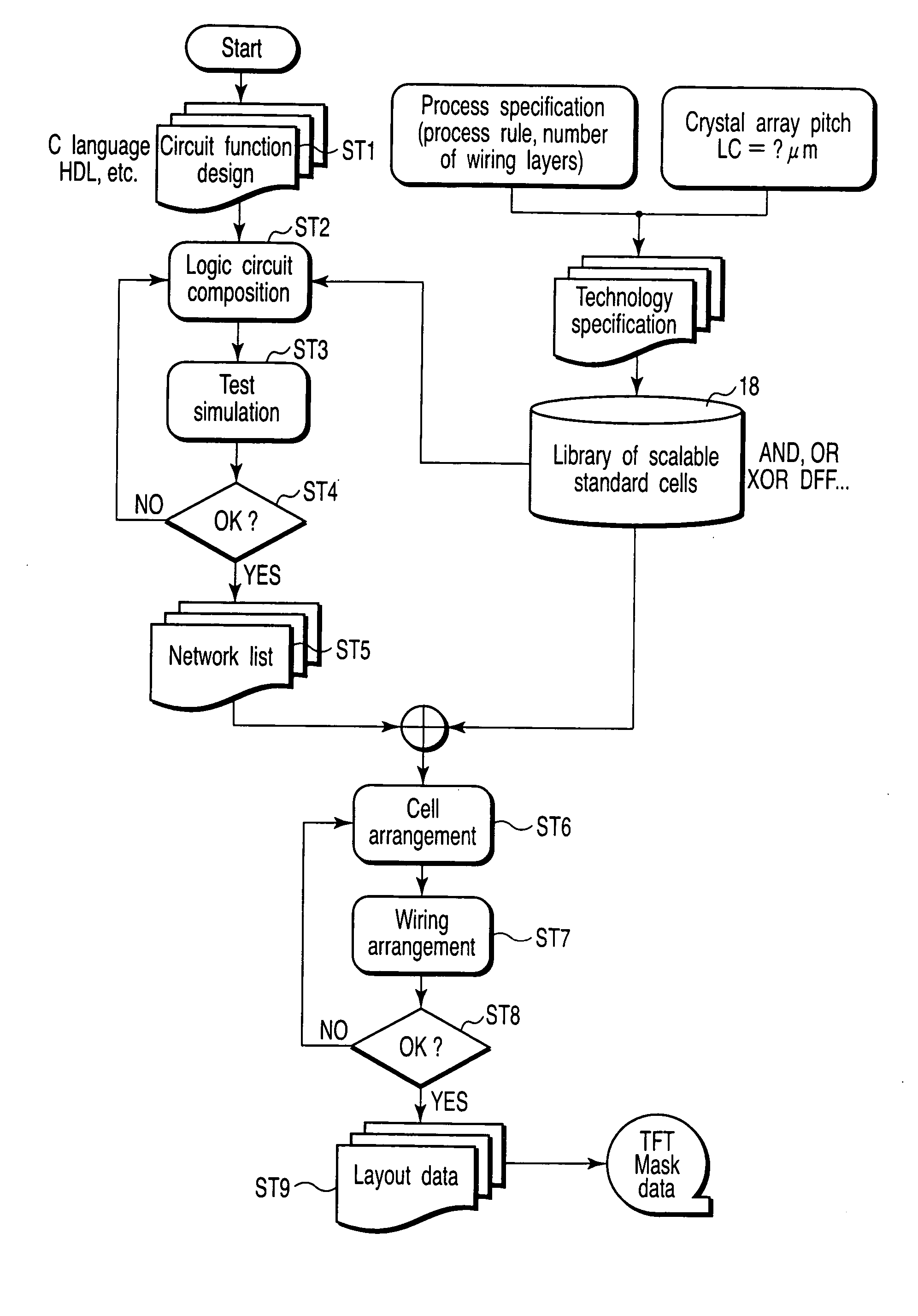
[0049] A thin-film transistor circuit according to an embodiment of the present invention will be described hereinafter with reference to the accompanying drawings.

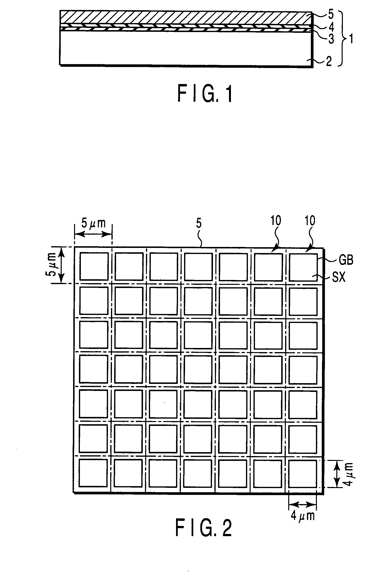
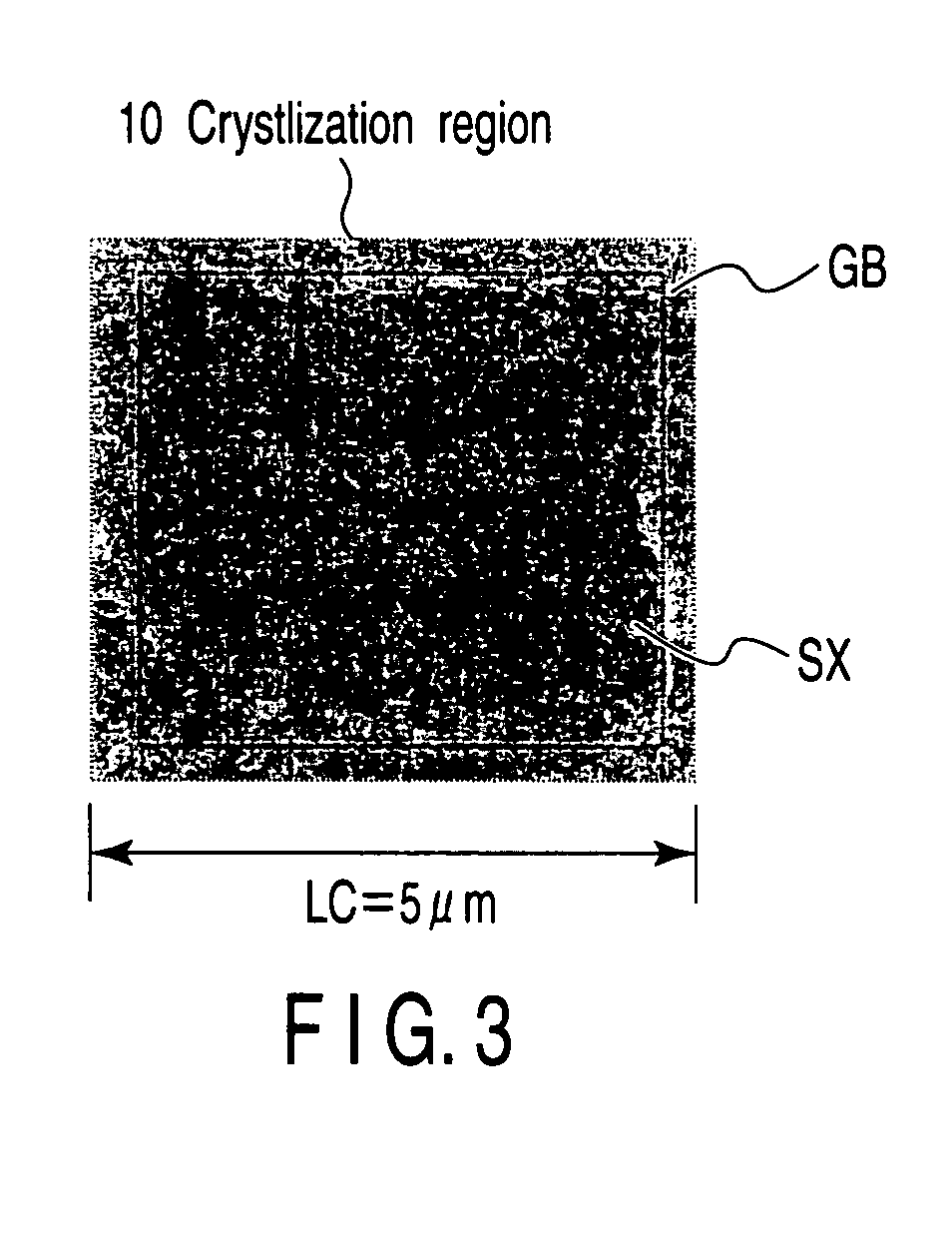
[0050]FIG. 1 shows a sectional structure of a thin-film semiconductor substrate 1 used in manufacturing the thin-film transistor circuit, and FIG. 2 shows a planar structure of the thin-film semiconductor substrate 1. The thin-film semiconductor substrate 1 is composed of a transparent dielectric substrate 2 such as of no-alkali glass, an SiNx film 3 formed on the transparent dielectric substrate 2, an SiO2 film 4 formed on the SiNx film, and a crystallized semiconductor thin film 5. The crystallized semiconductor thin film 5 is obtained, for example, by crystallizing an amorphous silicon film, and comprises crystal grains SX arrayed at regularly spaced intervals in the form of a matrix and amorphous silicon or polycrystalline silicon of fine grain size to surround the crystal grains SX. That is, the crystallized semicon...


PUM


Abstract

A thin-film transistor circuit includes a crystallized semiconductor thin film two-dimensionally partitioned into crystal-grain-defining areas each of which accommodates a crystal grain larger than a predetermined size, thin-film transistors each of which has a channel region placed at the center position of a corresponding one of the crystal-grain-defining areas, and wirings which interconnect the thin-film transistors.

Description

CROSS-REFERENCE TO RELATED APPLICATIONS [0001] This application is based upon and claims the benefit of priority from prior Japanese Patent Applications No. 2004-172647, filed Jun. 10, 2004; and No. 2005-138732, filed May 11, 2005, the entire contents of both of which are incorporated herein by reference. BACKGROUND OF THE INVENTION [0002] 1. Field of the Invention [0003] The present invention relates to a thin-film transistor circuit that uses a crystallized semiconductor thin film having crystal grains of relatively large size, a design method for the thin-film transistor circuit, a design program for the thin-film transistor circuit, a design program recording medium, a design library database, and a display device. [0004] 2. Description of the Related Art [0005] Flat-panel display devices have found use in various fields because of their features of thinness, lightness, and low power dissipation. Above all, active-matrix flat-panel display devices have been widely used in OA equ...

Claims


Application Information

Patent Timeline
IPC IPC(8): G02F1/1368G06F17/50G06F19/00H01L21/20H01L21/82H01L29/786
CPCG06F17/5072G06F17/5077Y02B60/1225G06F2212/2022G06F2212/1028G06F30/394G06F30/392Y02D10/00
Inventor KAWACHI, GENSHIRO
Owner SHARP KK
Why Eureka
Try Eureka