Method of physical planning voltage islands for ASICs and system-on-chip designs

a technology of voltage islands and asics, applied in the field of automatic design of integrated circuit chips, can solve the problems of reducing circuit performance, power consumption becoming a critical design metric, and difficulty in meeting the timing requirements of modem system-on-a-chip designs, and achieve the effect of minimizing the overall power consumption of the design

Inactive Publication Date: 2005-12-15
GOOGLE LLC
View PDF5 Cites 38 Cited by
  • Summary
  • Abstract
  • Description
  • Claims
  • Application Information

AI Technical Summary

Benefits of technology

[0012] In a first aspect of the invention, there is provided a method of generating a partitioning of an input design netlist, such that each partition corresponds to a voltage island running at a specific voltage, and such that the overall power consumption of the design is minimized.

Problems solved by technology

While meeting the timing requirements of modem System-on-a-Chip (SoC) designs is difficult, power consumption has become a critical design metric due to increasing power density and the wide use of portable systems.
However, lowering VDD leads to a reduced circuit performance, the amount of reduction being bound by the delay on the critical path which leaves most non-critical paths having a large slack.
The main problem when using multiple supplies is the distribution of power to the various voltage supplies.
In a grid-style power distribution network, a fine-grained approach, such as a gate-based one is extremely difficult to achieve.
This approach, while alleviating the problem of power distribution in the fine grained approach presents several problems such as: identifying partitions of circuits for a VDD assignment; characterizing each partition with respect to VDD; and floorplanning partitions such that those powered by the same VDD are grouped together.
However, its application is limited because partitions and floorplanning are assumed to be given.
If partitioning and floorplanning are not performed intelligently, the design space becomes significantly narrow.
The number of partitions it can handle is limited as well, since the complexity of the approach grows exponentially.
These, however, are still limited to using two VDDs instead of many VDDs.
Introducing voltage islands complicates the chip design process even more with respect to static timing, power routing, floorplanning, and the like.
The complexity grows significantly with the number of islands.
Since each island requires its own power grid and level converters to communicate with different islands, the overhead related to area and delay becomes unavoidable.
Additional area overhead may become available when using dead spaces when two or more cores are placed in the same island, although they cannot always be packed effectively.
These problems have not been addressed in prior works in related areas.

Method used


Image

  • Method of physical planning voltage islands for ASICs and system-on-chip designs
  • Method of physical planning voltage islands for ASICs and system-on-chip designs
  • Method of physical planning voltage islands for ASICs and system-on-chip designs

Examples


Embodiment Construction

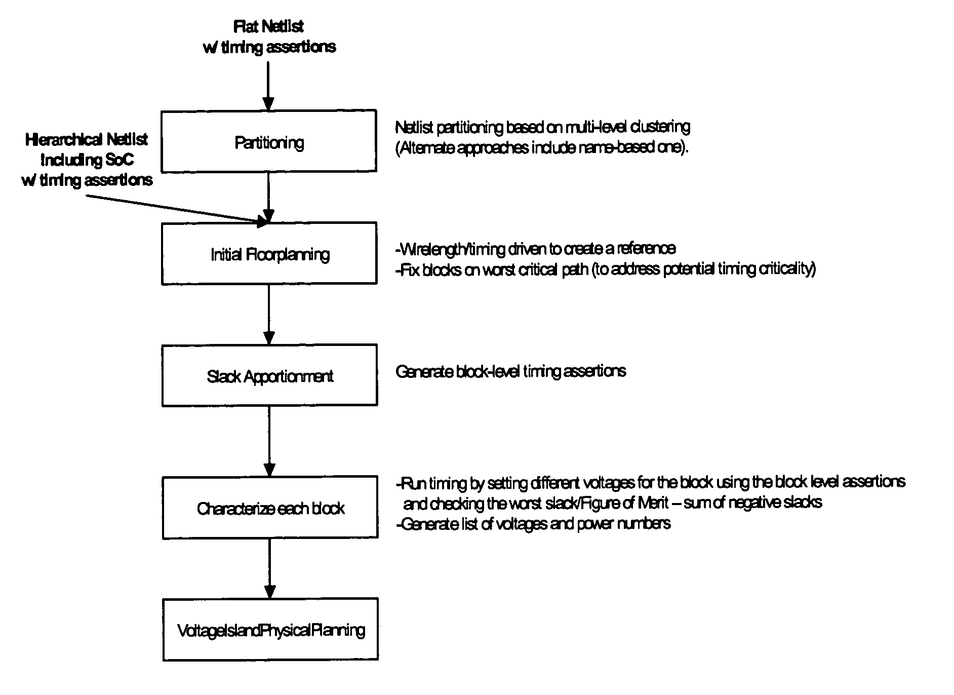
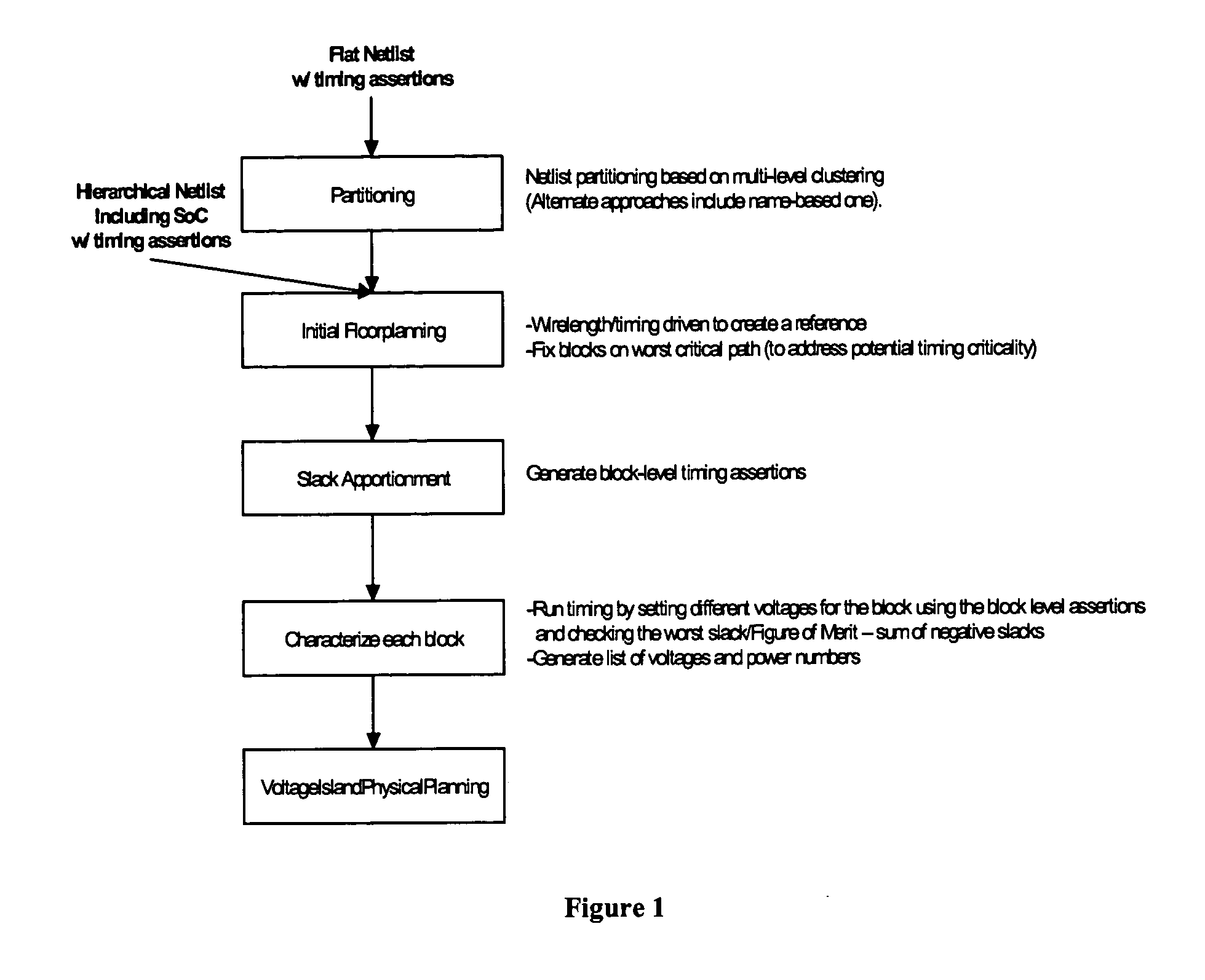
[0022]FIG. 1 shows the outline of the overall design flow when using the voltage island physical planning methodology of the present invention. If the netlist is flat, partitioning is performed such that each partition consists of only latch-to-latch paths. The result of this partitioning process consists of clusters of cells. This is achieved by first identifying the latches that are closest to the primary outputs (POs) followed by creating fan-in cones for each latch. This process is repeated for latches closest to the fan-in cones thus generated, and continued until the primary inputs (PIs) are reached. Since many such fan-in cones and overlaps between them exist, it becomes necessary to merge some of the cones based on the number of partitions required and the amount of logic that is cloned in the region of overlap.

[0023] If the input netlist is a SoC like design that is assembled from cores, then the inventive method uses the existing cores as the starting clusters upon which ...


PUM


Abstract

Voltage islands enable a core-level power optimization of ASIC / SoC designs by utilizing a unique supply voltage for each cluster of the design. Creating voltage islands in a chip design for optimizing the overall power consumption consists of generating voltage island partitions, assigning voltage levels and floorplanning. The generation of voltage island partitions and the voltage level assignment are performed simultaneously in a floorplanning context due to the physical constraints involved. This leads to a floorplanning formulation that differs from the conventional floorplanning for ASIC designs. Such a formulation of a physically aware voltage island partitioning and method for performing simultaneous voltage island partitioning, level assignment and floorplanning are described, as are the definition and the solution of floorplanning for voltage island based designs executed under area, power, timing and physical constraints. The physical planning of voltage islands includes: a) characterizing cell clusters in terms of voltages and power consumption values; b) providing a set of cell clusters that belong to a single voltage island Random Logic Macro (RLM); and c) assigning voltages for the voltage island RLMs, all within the context of generating a physically realizable floorplan for the design.

Description

BACKGROUND OF THE INVENTION [0001] The present invention is related to the automated design of integrated circuit (IC) chips and, more particularly, to a method of physical planning voltage islands applicable to ASICs and System-on-a-Chip designs. [0002] While meeting the timing requirements of modem System-on-a-Chip (SoC) designs is difficult, power consumption has become a critical design metric due to increasing power density and the wide use of portable systems. Many techniques are available for reducing power consumption, of which one of the most effective ones consists in lowering the voltage (VDD) because power consumption due to switching is proportional to VDD2 and the standby power consumption is proportional to VDD. However, lowering VDD leads to a reduced circuit performance, the amount of reduction being bound by the delay on the critical path which leaves most non-critical paths having a large slack. [0003] A dual VDD approach has been described by K. Usami, et al., in...

Claims


Application Information

Patent Timeline
Patent Type & Authority Applications(United States)
IPC IPC(8): G06F9/45G06F17/50
CPCG06F17/5068G06F30/39
Inventor DHANWADA, NAGASHYAMALA R.SHIN, YOUNGSOOHU, JINGCAO
Owner GOOGLE LLC
Why Eureka
Try Eureka