Integrated circuit chip manufacturing method and semiconductor device

a manufacturing method and integrated circuit technology, applied in semiconductor devices, semiconductor device details, electrical apparatus, etc., can solve the problems of difficult to hold a chip during die bonding, patent reference 2 does not disclose the formation of chips from the semiconductor device placed on the diamond substrate, etc., to facilitate dicing and die bonding, the effect of facilitating the formation of chips

Active Publication Date: 2005-12-22
CANON KK
View PDF6 Cites 14 Cited by
  • Summary
  • Abstract
  • Description
  • Claims
  • Application Information

AI Technical Summary

Benefits of technology

[0009] The present invention has been made on the recognition of the above problems, and has as its object to moderate the difficulty in chip formation or packagi

Problems solved by technology

However, patent reference 2 does not disclose forming chips from the semiconductor device placed on the diamond substrate.
Thinning of the s

Method used


Image

  • Integrated circuit chip manufacturing method and semiconductor device
  • Integrated circuit chip manufacturing method and semiconductor device
  • Integrated circuit chip manufacturing method and semiconductor device

Examples


first embodiment

[First Embodiment]

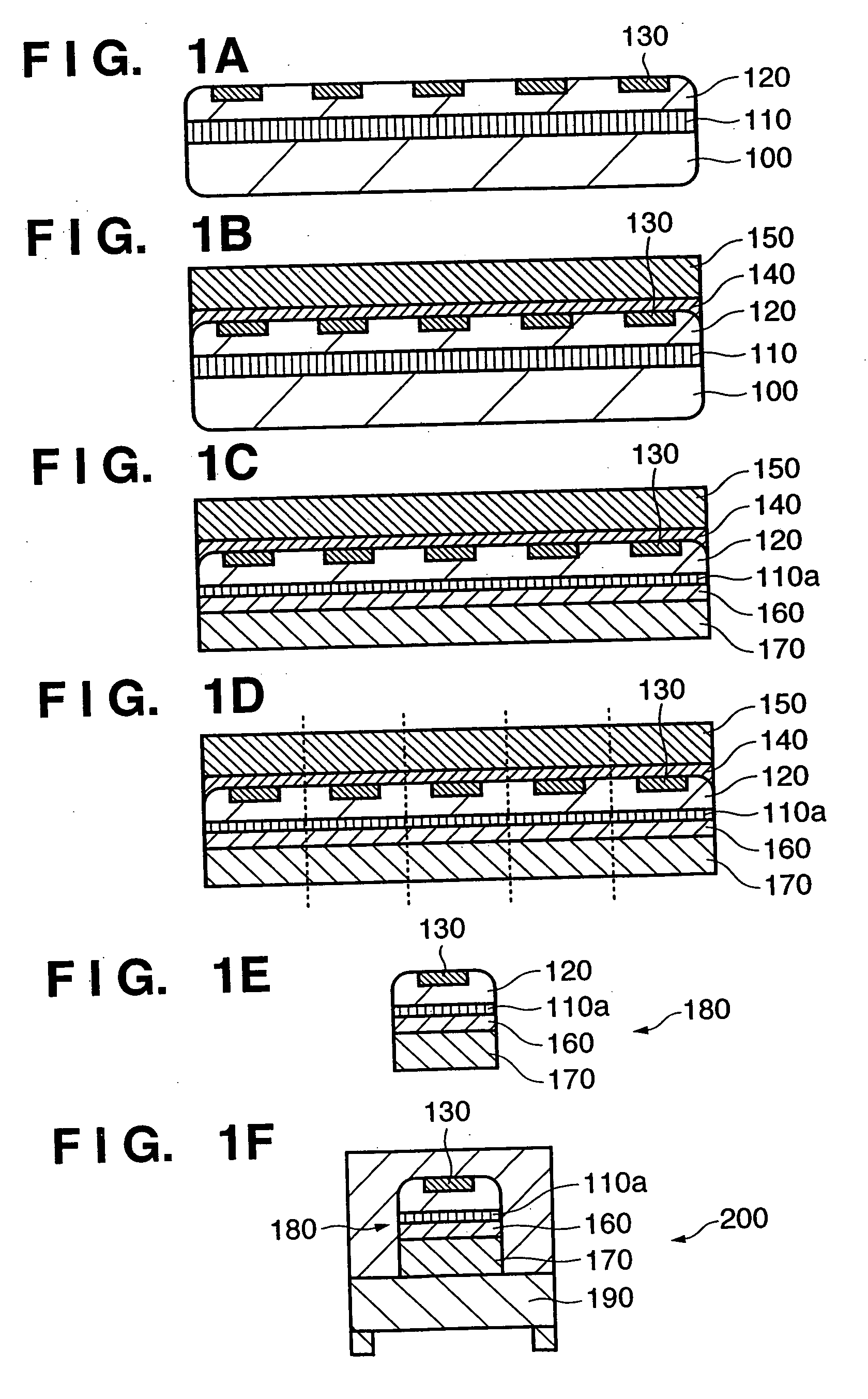
[0036] The first embodiment of the present invention will be described with reference to FIGS. 1A to 1F.

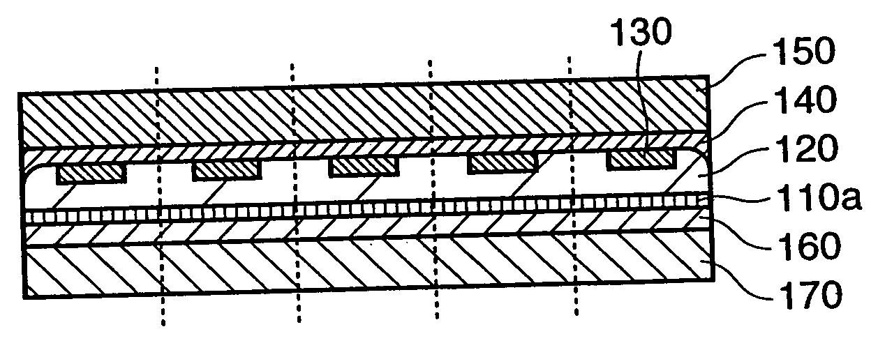
[0037] First, in the step shown in FIG. 1A, a separation layer 110 and semiconductor layer (semiconductor region) 120 are formed on a semiconductor substrate 100 serving as a seed substrate. Then, integrated circuits 130 including semiconductor devices are formed in the semiconductor layer 120.

[0038] More specifically, a porous layer 110 including two layers having different porosities is formed as a separation layer on the silicon substrate (semiconductor substrate) 100 serving as the seed substrate by an anodizing process. The porous layer 110 including the two layers having the different porosities can be formed by changing conditions (e.g., current conditions) for the anodizing process. When the porous layer 110 including the two layers having the different porosities is formed, the interface between the two layers can be used as a separation interface in a...

second embodiment

[Second Embodiment]

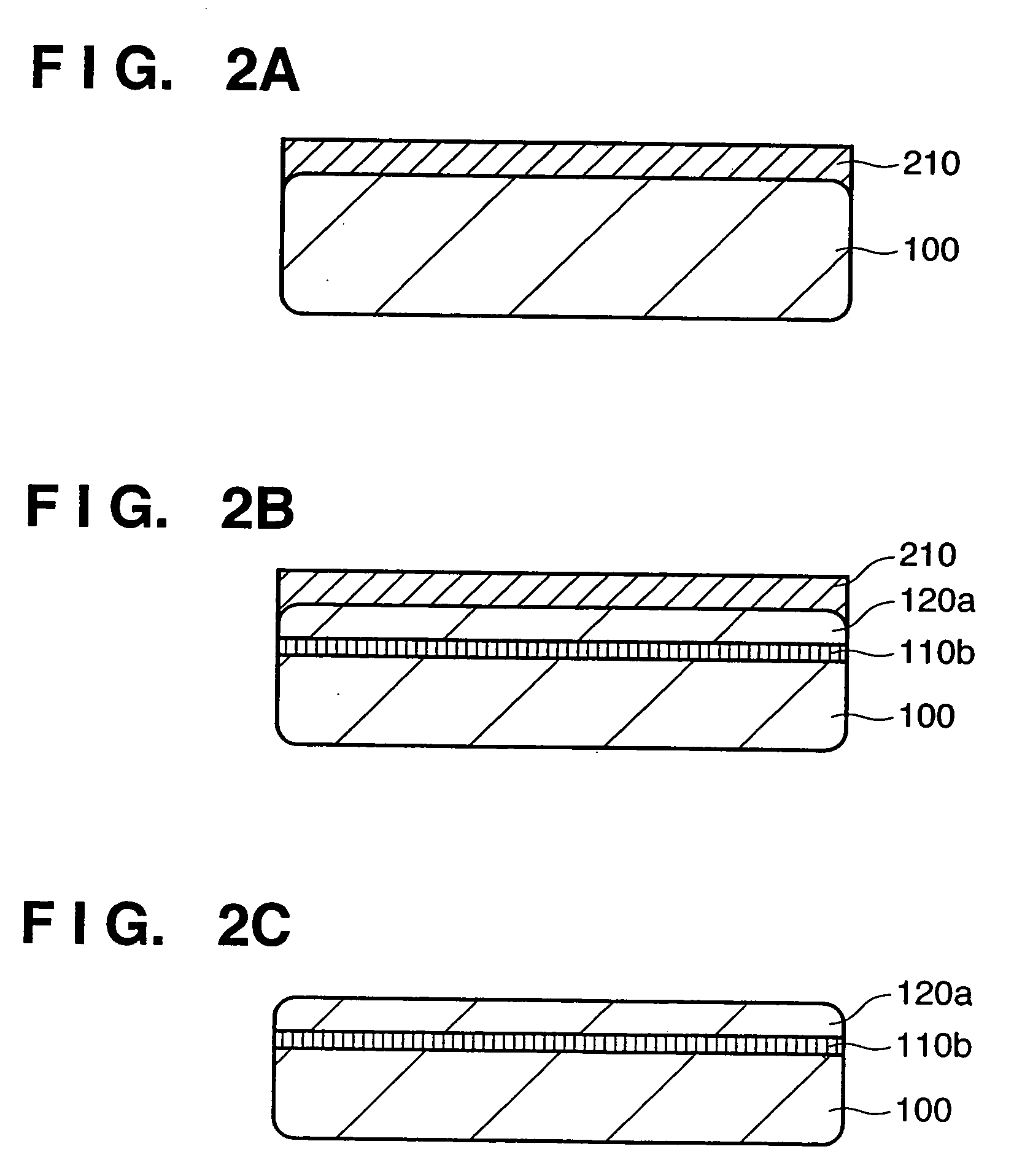
[0075] According to the second embodiment, the method of forming the separation layer of the first embodiment is changed.

[0076] First, in the step shown in FIG. 2A, an insulating layer (e.g., a SiO2 layer) serving as a protection film 210 is formed on a silicon substrate (semiconductor substrate) 100 serving as a seed substrate. In the step shown in FIG. 2B, ions such as hydrogen ions are implanted in the silicon substrate 100 to form an ion-implanted layer serving as a separation layer (ion-implanted layer) 110b in a region at a predetermined depth from the surface of the silicon substrate 100. For example, the implantation amount of the hydrogen ions can be set to the order of 1016 to 1017 (atoms / cm2).

[0077] After that, the protection film 210 is removed in the step shown in FIG. 2C. Thus, a substrate which has semiconductor layer 120a on the separation layer 110b an be formed. The substrate obtained in this manner is subjected to the steps shown in FIGS. 1B t...

third embodiment

[Third Embodiment]

[0079] This embodiment provides an optical card manufacturing method as well as a method of removing a seed substrate without using a separation layer.

[0080] First, integrated circuits including, e.g., a light-receiving element and amplification circuit, are formed on a silicon substrate serving as a seed substrate. After that, the first support member is bonded to the silicon substrate such that the integrated circuit side (first surface side) becomes inside.

[0081] Subsequently, the silicon substrate is thinned from the lower surface (second surface side) by grinding and abrasion using a grinder to leave a semiconductor layer (semiconductor region) having a predetermined thickness (e.g., 50 μm) as a region that includes integrated circuits.

[0082] Subsequently, a light-transmitting substrate (quartz substrate) serving as the second support member is bonded to the integrated circuit side (second surface side) of the obtained substrate. In this case, annealing (e....


PUM


Abstract

This invention moderates the difficulty in chip formation or packaging which accompanies thinning of a semiconductor region where an integrated circuit is formed. An integrated circuit chip manufacturing method includes a first bonding step of bonding a first support member to a first surface of a semiconductor substrate which has the first surface and a second surface and has a semiconductor region including an integrated circuit on a first surface side thereof, a thinning step of removing a second surface-side portion of the semiconductor substrate bonded to the first support member to leave the semiconductor region, thereby thinning the semiconductor substrate, a second bonding step of bonding a second support member to the second surface side of the thinned semiconductor substrate, and a chip forming step of forming chips by cutting the semiconductor region.

Description

FIELD OF THE INVENTION [0001] The present invention relates to an integrated circuit chip manufacturing method and semiconductor device. BACKGROUND OF THE INVENTION [0002] In recent years, a technique which thins a semiconductor device attracts attention. According to the technique disclosed in patent reference 1, a protection film, protection insulating layer, and thin film layer are sequentially formed on the first substrate. The second substrate is adhered to the tin film layer with an adhesive. After that, the first substrate is removed by etching. The protection film is further removed to expose the protection insulating layer. A protection substrate is adhered to the protection insulating layer with an adhesive. After that, flexible cables are connected to the electrode portions of the thin film layer to manufacture an active matrix type organic electroluminescence display. Patent reference 1 is aimed at manufacturing a large-area thin film layer which is to be used as a displ...

Claims


Application Information

Patent Timeline
IPC IPC(8): H01L21/68H01L21/762H01L21/78H01L23/12
CPCH01L21/6835H01L21/6836H01L21/76256H01L2221/6834H01L2221/68318H01L2221/68327H01L21/78Y10S438/977
Inventor MOMOI, KAZUTAKASATO, NOBUHIKO
Owner CANON KK
Why Eureka
Try Eureka