
Thermal interposer for thermal management of semiconductor devices

a technology of thermal management and semiconductor devices, applied in semiconductor devices, semiconductor/solid-state device details, electrical apparatus, etc., can solve the problems of inability to rigidly join to the integrated circuit chip, and inability to achieve thermal conductivity high

Inactive Publication Date: 2005-12-22
IBM CORP
View PDF11 Cites 62 Cited by
  • Summary
  • Abstract
  • Description
  • Claims
  • Application Information

AI Technical Summary

Benefits of technology

[0020] Yet another embodiment of the present invention provides an integrated circuit device that includes a semiconductor device having a front surface containing active devices and a back surface that does not contain active devices, an upper plate having a bottom surface with a recess and a top surface, and a lower plate having a top surface with a recess and a bottom surface. The semiconductor device is made of a material having a coefficient of thermal expansion, the upper plate is made of a material having high thermal conductivity, and the lower plate is made of a material having a coefficient of thermal expansion that is substantially the same as the coefficient of thermal expansion of the material of which the semiconductor device is made. The bottom surface of the upper plate is hermetically bonded to the top surface of the lower plate so that a vapor chamber is formed by the recesses in the upper and lower plates, and the back surface of the semiconductor device is bonded to the bottom surface of the lower plate. At least a top surface of the recess in the upper plate and at least a bottom surface of the recess in the lower plate are lined with graphite foam.

Problems solved by technology

Insufficient transfer of heat away from an electronic device can result in performance and reliability degradation of that device or circuit due to an unacceptably high operating temperature.
However, such a conventional vapor chamber is typically fabricated out of metal.
Thus, it cannot be rigidly joined to the integrated circuit chip due to a thermal expansion mismatch.
As with a conventional vapor chamber structure, because the heat pipe is fabricated from a metal (such as copper), it cannot be rigidly joined to an integrated circuit chip due to a thermal expansion mismatch.
However, this structure is very complicated and presents practical disadvantages such as difficulty in electrically connecting and reworking the chips.
However, a disadvantage of such a structure is that the wick is only provided on one surface of the interior cavity of the vapor chamber.
However, such a structure is complicated and its performance is limited because the fluid return is only around the perimeter region.
However, such a structure would be difficult to implement using either of the silicon vapor chamber structures described above.
Further, metallic vapor chambers present the disadvantages described above.

Method used


Image

  • Thermal interposer for thermal management of semiconductor devices
  • Thermal interposer for thermal management of semiconductor devices
  • Thermal interposer for thermal management of semiconductor devices

Examples


first embodiment

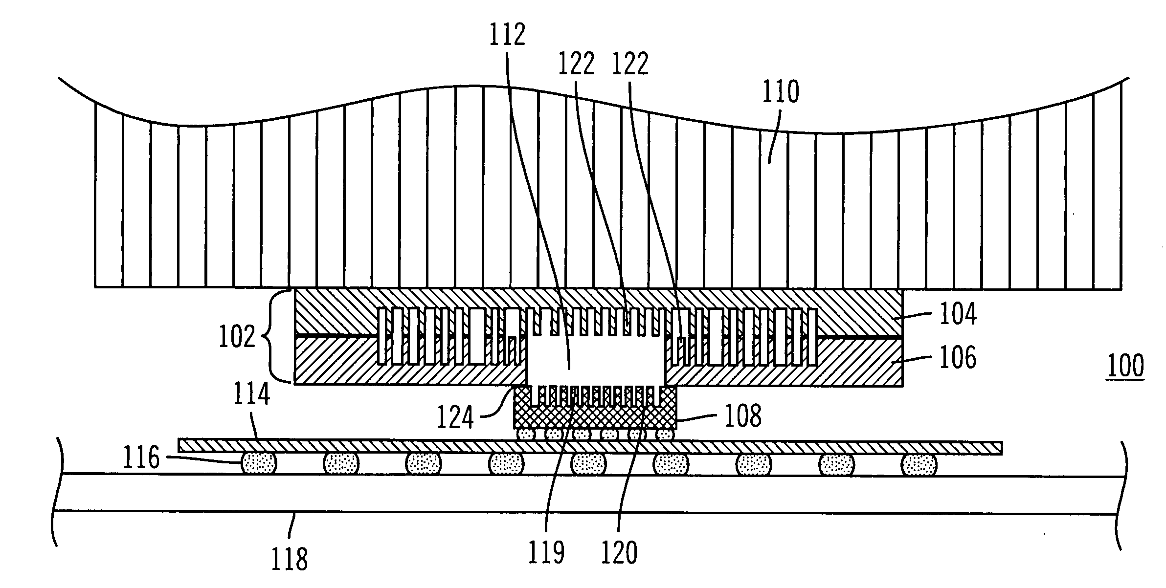
[0045]FIG. 1 illustrates a cross sectional diagram of an integrated thermal interposer according to the present invention. The wick structures (or grooves) 120 and 122 are shown in FIG. 1 as being composed of parallel and evenly spaced channels and fins so that the overall structure can be easily understood. However, as will become apparent from subsequent drawings, the configuration of the wick structure in preferred embodiments is significantly more complicated.

[0046] As shown in FIG. 1, a semiconductor device 108 has a back surface 119 a wick structure (such as grooves) 120. The integrated thermal interposer 102 has two plates 104 and 106, both having a wick structure 122. These two plates 104 and 106 are bonded together with the wick structures facing each other by soldering, brazing, direct silicon bonding or any other appropriate bonding method that forms a suitable hermetic seal. The upper plate 104 is made of a thermally conductive material, such as silicon, silicon carbide,...

second embodiment

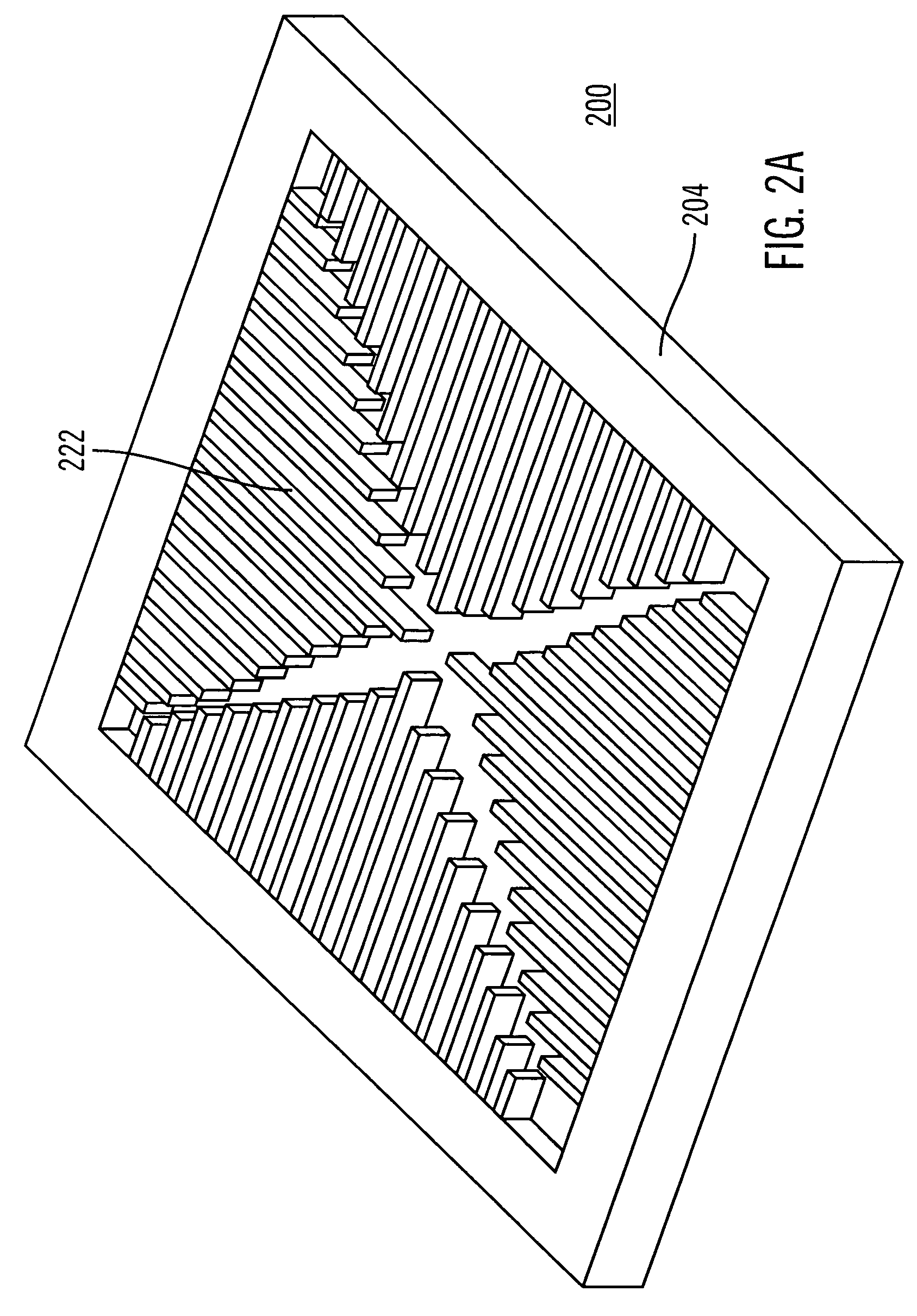
[0056]FIG. 3B illustrates a cross sectional view of a portion of the grooves and walls of an upper plate of a thermal interposer according to the present invention. In this embodiment, a section of the wick structure (e.g., grooves) and walls 304 of the upper plate and / or the lower plate are covered with a layer 322 of graphite foam, graphite fiber, or carbon nanotubes. More specifically, the upper plate 104 and / or the lower plate 106 are made of silicon, and the surfaces of the wick structure are further processed so as to deposit or otherwise add anisotropic graphite foam, graphite fiber, or carbon nanotubes onto them. In various embodiments, the graphite foam, graphite fiber, or carbon nanotubes 322 cover some or all of the wick structures. This added layer 322 of material greatly increases the surface area so as to provide increased wicking action to return the working fluid to the semiconductor chip where it is vaporized. Further, the high thermal conductivity of the graphite f...

third embodiment

[0061]FIG. 4 illustrates a cross sectional diagram of an integrated thermal interposer having one plate according to the present invention. As shown, a single plate 404 with grooves 422 is bonded directly to the back surface of a semiconductor device 408. The grooved (or other wick structured) portion 424 of the plate is dimensioned so as to be over the area 426 of the back surface 409 of the semiconductor device 408. Once the bonding areas of the plate 404 and the back surface of the semiconductor device 408 are aligned and bonded together by use of a solder band or similar hermetic bonding material 406, they can be evacuated and filled with a suitable working fluid (e.g., via a fill port on the side or back of the plate 404) to form a vapor chamber structure. A heat-sink fixture can be thermally coupled to the top of the plate 404, as in the embodiment of FIG. 1. Additionally, a substrate can be attached to the bottom surface of the semiconductor device 408 for electrical connecti...


PUM


Abstract

A thermal interposer is provided for attachment to a surface of a semiconductor device. In one embodiment, the thermal interposer includes an upper plate having a bottom surface with a plurality of grooves and made of a material having high thermal conductivity, and a lower plate having a top surface with a plurality of grooves and made of a material having a coefficient of thermal expansion that is substantially the same as the coefficient of thermal expansion of the material of a semiconductor device that is bonded to the bottom surface of the lower plate. The bottom surface of the upper plate is hermetically bonded to the top surface of the lower plate so that a vapor chamber is formed by the upper and lower plates, and walls of the grooves on the top surface of the lower plate extend to within less than 250 microns from walls of the grooves on the bottom surface of the upper plate comprise a plurality of second walls the first walls.

Description

CROSS-REFERENCE TO RELATED APPLICATIONS [0001] This application is related to the inventors' application “THERMAL INTERPOSER FOR THERMAL MANAGEMENT OF SEMICONDUCTOR DEVICES,” Ser. No. ______, now ______, which was filed on the same day as the present application and commonly assigned herewith to International Business Machines Corporation. This related application is incorporated herein by reference.BACKGROUND OF THE INVENTION [0002] 1. Field of the Invention [0003] This invention generally relates to the field of electronic devices, and more specifically to thermal interposers, or heat spreaders, for thermal management and cooling of semiconductor devices. [0004] 2. Description of Related Art [0005] Thermal management is of great importance to the operation of electronic devices. Thermal management is especially important in the operation of semiconductor devices as factors such as increasing operating frequencies push power consumption, and therefore heat generation, to the limits...

Claims


Application Information

Patent Timeline
Patent Type & Authority Applications(United States)
IPC IPC(8): H01L23/02H01L23/427
CPCH01L23/427H01L2224/16H01L2224/73253H01L2924/01078H01L2224/16225H01L2924/10158H01L2924/15311H01L2924/01019H01L2924/01322H01L2924/09701
Inventor MOK, LAWRENCE S.COLGAN, EVAN G.LU, MINHUASHIH, DA-YUAN
Owner IBM CORP
Features
  • Generate Ideas
  • Intellectual Property
  • Life Sciences
  • Materials
  • Tech Scout
  • Unparalleled Data Quality
  • Higher Quality Content
  • 60% Fewer Hallucinations
Learn More