Al technical title is built by PatSnap Al team. It summarizes the technical point description of the patent document.
a logic driver and nanotube technology, applied in logic circuit coupling/interface arrangement, pulse technique, instruments, etc., can solve the problems of high power consumption, density and operation speed of mos digital circuits, and limited density of bipolar digital integrated circuits
Inactive Publication Date: 2005-12-22
NANTERO
View PDF34 Cites 55 Cited by
Summary
Abstract
Description
Claims
Application Information
AI Technical Summary
This helps you quickly interpret patents by identifying the three key elements:
Problems solved by technology
Method used
Benefits of technology
[0031] Under another aspect of the invention, the off-chip driver circuit further includes a second switching element having an input node, an output node, a nanotube channel element, and a control structure disposed in relation to the nanotube channel element to controllably form and unform an electrically conductive channel between said input node and said output node; and further comprising a second output link connectable to a second off-chip impedance load. The input node of the second switching element is coupled to a reference signal and the control structure of the second switching element is coupled to the first and second signal links. The output node of the second switching element is coupled to the second output link, and the nanotube channel element of the second switching element is sized to carry sufficient current to drive the off-chip impedance load.
[0032] Under another aspect of the invention, an off-chip driver circuit includes a differential input having a first and second signal links, each coupled to a respective one of two differential, on-chip signals. At least one output link is connectable to an off-chip impedance load. At least first and second switching elements each have an input node, an output node, a nanotube channel element, and a control structure disposed in relation to the nanotube channel element to controllably form and unform an electrically conductive channel between said input node and said output node. The input node of the first switching element is coupled to a first reference signal and input node of the second switching element is coupled to a second reference signal. The control structure of each of the first and second switching elements is coupled to the first and second signal links and the output node of each of the first and second switching elements is coupled to the output link. The nanotube channel element of each of the first and second switching elements is sized to carry sufficient current to drive said off-chip impedance load.
[0033] Under another aspect of the invention, an off-chip driver circuit includes a differential input having a first and second signal links, each coupled to a respective one of two differential, on-chip signals. First and second output links are each connectable to an off-chip impedance load. The circuit further includes at least first and second push-pull drivers, each push-pull driver connected to the first and second input links and each connected to a respective one of the first and second output links. Each push-pull driver includes first and second switching elements, each having an input node, an output node, a nanotube ...
Problems solved by technology
However, the density of bipolar digital integrated circuits is limited by their high power consumption and the ability of packaging technology to dissipate the heat produced while the circuits are operating.
The density and operating speed of MOS digital circuits are still limited by the need to dissipate the heat produced when the device is operating.
Digital logic integrated circuits constructed from bipolar or MOS devices do not function correctly under conditions of high heat or heavy radiation.
As leakage current increases, the operating temperature of the device rises, the power consumed by the circuit increases, and the difficulty of discriminating the off state from the on state reduces circuit reliability.
Conventional digital logic circuits also short internally when sub...
Method used
Image
Click on the blue label to locate the original text in one second.
Reading with bidirectional positioning of images and text.
Examples
Embodiment Construction
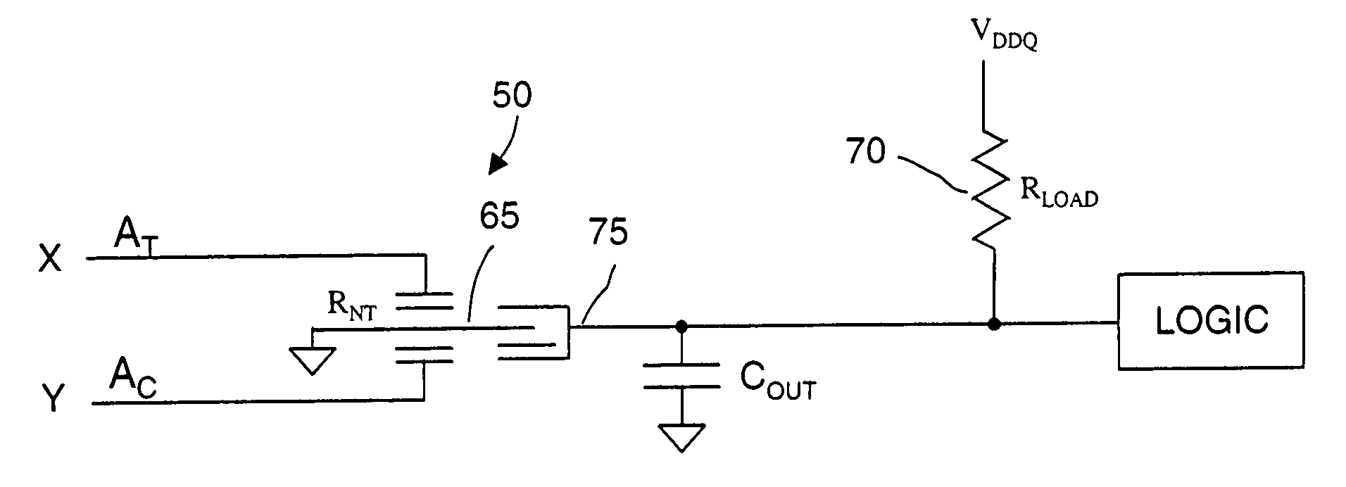
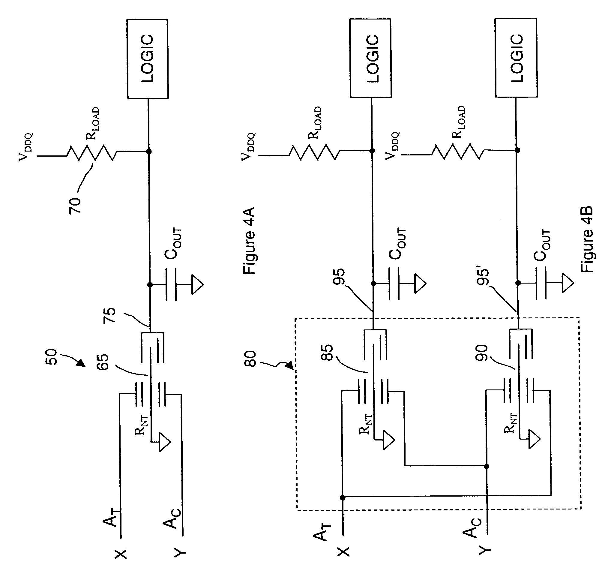
[0048] Preferred embodiments of the invention arrange nanotube-based switches into driver circuits capable of driving relatively large capacitances, such as off chip (OC) capacitances, long or heavily loaded interconnect lines, etc. The circuits may be either dual-rail (differential) or single-rail, open carbon nanotube (CNT) output (corresponds to open drain in an FET), push pull drivers, and tristate push pull drivers, for example.
[0049] Carbon nanotube-based logic circuits, such as those circuits disclosed in the incorporated, related references, may be required to drive a relatively large capacitance, 10 pf for example, when driving off-chip, or when driving heavy loads on-chip. Nanotube-based logic circuits using porous carbon nanotube fabrics to construct nanotube channel elements are typically low capacitance circuits, e.g., 30 aF (0.030 fF) input and output capacitances, and can typically drive only relatively low capacitances. Preferably, a logic family includes circuits t...
PUM
Abstract
Nanotube based logic driver circuits. These include pull-up driver circuits, push-pull driver circuits, tristate driver circuits, among others. Under one embodiment, an off-chip driver circuit includes a differential input having first and second signal links, each coupled to a respective one of two differential, on-chip signals. At least one output link is connectable to an off-chip impedance load, and at least one switching element has an input node, an output node, a nanotube channel element, and a control structure disposed in relation to the nanotube channel element to controllably form and unform an electrically conductive channel between said input node and said output node. The input node is coupled to a reference signal and the control structure is coupled to the first and second signal links. The output node is coupled to the output link, and the channel element is sized to carry sufficient current to drive said off-chip impedance load.
Description
CROSS-REFERENCE TO RELATED APPLICATIONS [0001] This application claims priority under 35 U.S.C. § 119(e) to U.S. Provisional Pat. Apl., Ser. 60 / 581,074, filed on Jun. 18, 2004, entitled Nonvolatile Carbon Nanotube Logic (NLOGIC) Off Chip Driver, which is incorporated herein by reference in its entirety. [0002] This application is related to the following references: [0003] U.S. patent application Ser. No. 10 / 917,794, filed on Aug. 13, 2004, entitled Nanotube-Based Switching Elements; [0004] U.S. patent application Ser. No. 10 / 918,085, filed on Aug. 13, 2004, entitled Nanotube-Based Switching Elements With Multiple Controls; [0005] U.S. patent application Ser. No. 10 / 918,181, filed on Aug. 13, 2004, entitled Nanotube Device Structure And Methods Of Fabrication; [0006] U.S. patent application Ser. No. 10 / 917,893, filed on Aug. 13, 2004, entitled Nanotube-Based Switching Elements And Logic Circuits; [0007] U.S. patent application Ser. No. 10 / 917,606, filed on Aug. 13, 2004, entitled Is...
Claims
Application Information
Patent Timeline
Application Date:The date an application was filed.
Publication Date:The date a patent or application was officially published.
First Publication Date:The earliest publication date of a patent with the same application number.
Issue Date:Publication date of the patent grant document.
PCT Entry Date:The Entry date of PCT National Phase.
Estimated Expiry Date:The statutory expiry date of a patent right according to the Patent Law, and it is the longest term of protection that the patent right can achieve without the termination of the patent right due to other reasons(Term extension factor has been taken into account ).
Invalid Date:Actual expiry date is based on effective date or publication date of legal transaction data of invalid patent.