Organic light emitting device and method for manufacturing the same

a light-emitting device and organic technology, applied in semiconductor devices, instruments, electrical devices, etc., can solve the problems of slow response time and narrow viewing angle, and achieve the effects of good on/off characteristics, high mobility and stability

Inactive Publication Date: 2008-07-03
SAMSUNG ELECTRONICS CO LTD
View PDF15 Cites 27 Cited by
  • Summary
  • Abstract
  • Description
  • Claims
  • Application Information

AI Technical Summary

Benefits of technology

[0012]For the optimized characteristics of the OLED, characteristics of the switching thin film transistor (“TFT”) and those of the driving TFT may be different from each other. In particular, the switching TFT may have a good on / off characteristic, and the driving TFT may have high mobility and stability for supplying sufficient current for driving the OLED.

Problems solved by technology

However, because the LCD is a passive display device, an additional backlight as a light source is needed, and the LCD has various problems such as a slow response time and a narrow viewing angle.

Method used


Image

  • Organic light emitting device and method for manufacturing the same
  • Organic light emitting device and method for manufacturing the same
  • Organic light emitting device and method for manufacturing the same

Examples


embodiment 1

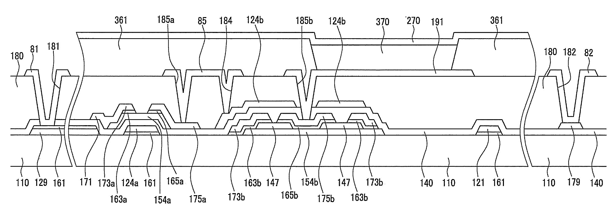
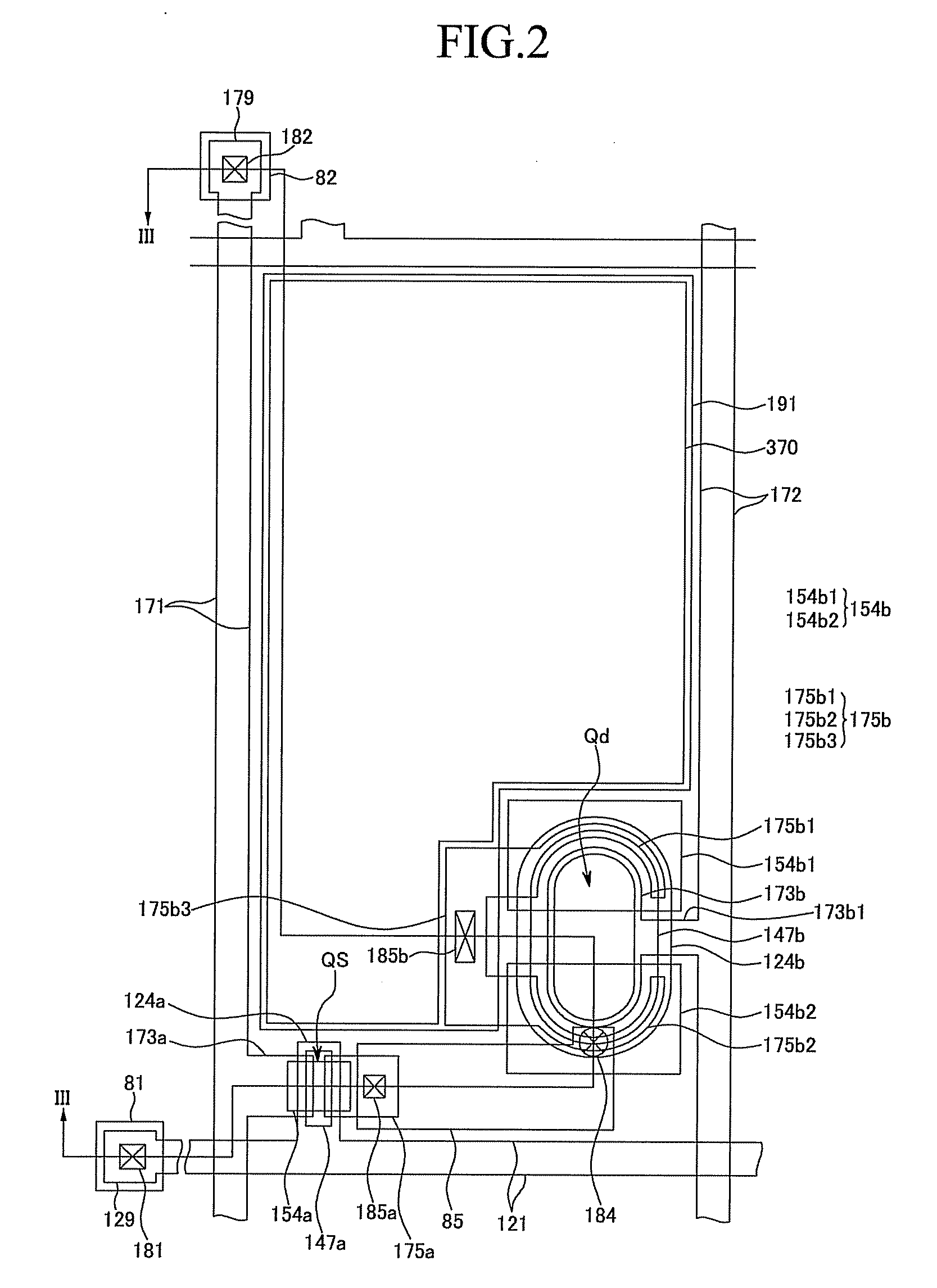
[0072]Referring to FIGS. 2 and 3, a detailed structure of the organic light emitting device shown in FIG. 1 according to an exemplary embodiment of the present invention will be described in detail.

[0073]FIG. 2 is a schematic plan view of an exemplary organic light emitting device according to an exemplary embodiment of the present invention, and FIG. 3 is a sectional view of the exemplary organic light emitting device shown in FIG. 2 taken along line II-II.

[0074]A plurality of switching and driving semiconductor islands 154a and 154b preferably made of microcrystalline silicon or polycrystalline silicon are formed on an insulating substrate 110 made of a material such as, but not limited to, transparent glass, quartz, or sapphire.

[0075]The switching and driving semiconductor islands 154a and 154b are separated from each other, and the driving semiconductor islands 154b include a first portion 154b1 and a second portion 154b2 that are separated from each other and are disposed in th...

embodiment 2

[0123]Referring to FIGS. 16 and 17, a detailed structure of an exemplary organic light emitting device shown in FIG. 1 according to another exemplary embodiment of the present invention will be described in detail.

[0124]FIG. 16 is an exemplary layout view of an exemplary organic light emitting device according to another exemplary embodiment of the present invention, and FIG. 17 is a sectional view of the exemplary organic light emitting device shown in FIG. 16, taken along line XVII-XVII. Detailed descriptions of elements having the same or substantially the same function as in the previous embodiments are omitted in this description of this embodiment according to the present invention for convenience of description.

[0125]A plurality of driving semiconductor islands 154b preferably made of crystalline silicon and including first and second portions 154b1 and 154b2 are formed on an insulating substrate 110, and a plurality of etch stoppers 147b preferably made of an insulating mate...

embodiment 3

[0151]Referring to FIGS. 32 and 33, a detailed structure of an exemplary organic light emitting device shown in FIG. 1 according to another exemplary embodiment of the present invention will be described in detail.

[0152]FIG. 32 is an exemplary layout view of an exemplary organic light emitting device according to another exemplary embodiment of the present invention, and FIG. 33 is a sectional view of the exemplary organic light emitting device shown in FIG. 32, taken along line XXXIII-XXXIII. Detailed descriptions of elements having the same or substantially the same function as in the previous embodiments are omitted in this description of this embodiment according to the present invention, for convenience of description.

[0153]A plurality of driving semiconductor islands 154b including first and second portions 154b1 and 154b2 are formed on an insulating substrate 110, and a plurality of etch stoppers 147b having a running oval shape are formed thereon.

[0154]A plurality of driving...


PUM


Abstract

An organic light emitting device includes a substrate, first and second signal lines formed on the substrate, a switching thin film transistor (“TFT”) connected to the first and second signal lines and including a first semiconductor, a driving TFT including a second semiconductor, an etch stopper formed on the second semiconductor, driving input and driving output electrodes overlapping the etch stopper and the second semiconductor and opposite to each other with respect to the etch stopper, and a driving control electrode connected to the switching TFT and overlapping the second semiconductor, a first electrode connected to the driving output electrode, a second electrode opposite to the first electrode, and an organic light emitting member, wherein at least one of the etch stopper, the driving input electrode, and the driving output electrode is symmetrical with respect to one straight line.

Description

[0001]This application claims priority to Korean Patent Applications Nos. 10-2006-0136160 filed on Dec. 28, 2006, and 10-2007-0028460 filed on Mar. 23, 2007, and all the benefits accruing therefrom under 35 U.S.C. §119, and the contents of which in their entireties are herein incorporated by reference.BACKGROUND OF THE INVENTION[0002](a) Field of the Invention[0003]The present invention relates to an organic light emitting device and a method for manufacturing the same. More particularly, the present invention relates to an organic light emitting device improving electrical characteristics thereof, and a method for manufacturing the organic light emitting device.[0004](b) Description of the Related Art[0005]Recent trends toward lightweight and thin personal computers and televisions sets also require lightweight and thin display devices, and flat panel displays such as a liquid crystal display (“LCD”) satisfying such a requirement are being substituted for conventional cathode ray t...

Claims


Application Information

Patent Timeline
Patent Type & Authority Applications(United States)
IPC IPC(8): G09G3/10H01L21/84H01L29/04
CPCH01L27/1214
Inventor HUH, JONG-MOO
Owner SAMSUNG ELECTRONICS CO LTD
Why Eureka
Try Eureka