
Heat treatment jig for silicon semiconductor substrate

a silicon semiconductor substrate and heat treatment technology, applied in the direction of charging supports, lighting and heating apparatus, furniture, etc., can solve the problems of thermally oxidized film being hindered, the thickness of the jig is thinner, and the heat treatment jig to date cannot fully meet the requirement of preventing the generation of slips, so as to reduce the surface steps, reduce the effect of slip generation, and reduce the thickness

Active Publication Date: 2005-12-22
SUMITOMO MITSUBISHI SILICON CORP
View PDF5 Cites 377 Cited by
  • Summary
  • Abstract
  • Description
  • Claims
  • Application Information

AI Technical Summary

Benefits of technology

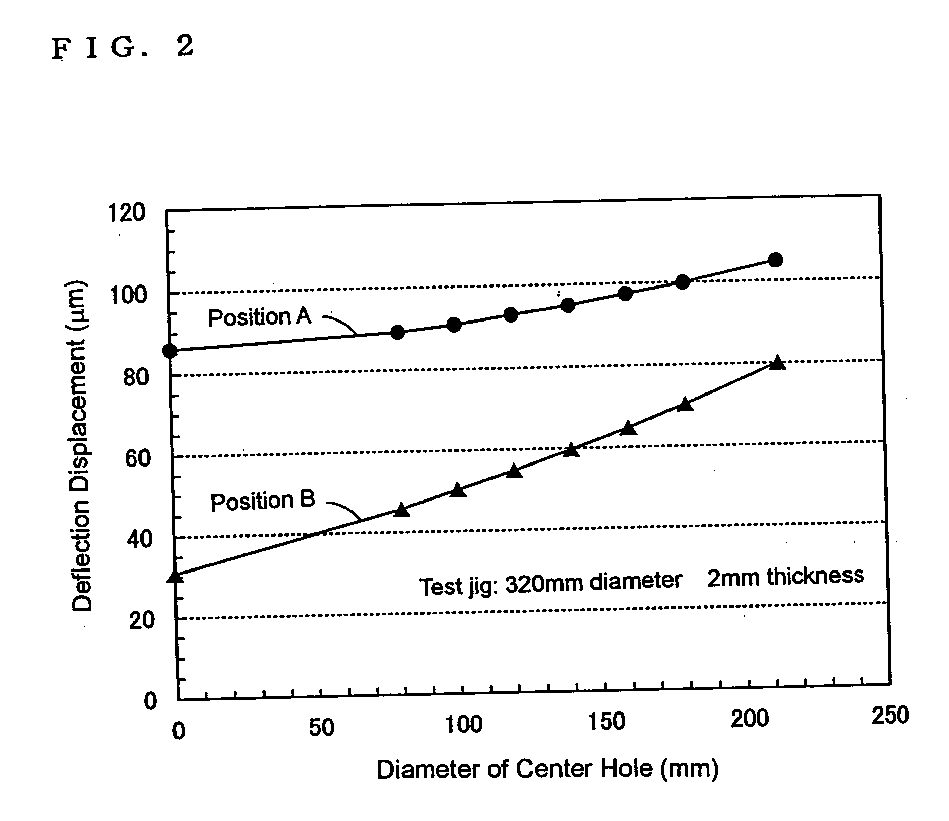
[0020] The present invention was made to solve above-mentioned problem in association with high temperature heat treatment for silicon semiconductor substrates and intends to provide a heat treatment jig enabling to effectively reduce the generation of the slips as well as to retard the generation of surface steps owing to the difference of developed thermally oxidized film on the back surface of said silicon substrate by applying followings; a deflection displacement of heat treatment jig in the state of being loaded onto a heat treatment boat in a vertical heat treatment furnace, is controlled; and the surface roughness at the region where to come into contact with the back surface of silicon substrate is vigorously investigated and adapted to be the proper range.
[0021] Thus, to achieve above-mentioned object, the present inventors carried out heat treatment extensively by applying for a heat treatment boat in a vertical heat treatment furnace, and made investigations as to the required configuration of heat treatment jig so that the generation of the slips is effectively retarded and the growth of thermally oxidized film is not hindered.
[0022] Conventionally, as a measure to retard the generation of the slips generation, it is perceived that it has been effective to control the flatness of heat treatment jig after machining. Accordingly, it has been stipulated that the flatness (JIS B 0621) at the region where to come into contact with silicon semiconductor substrates shall be controlled to be 100 μm or less, preferably 50 μm or less.
[0023] Nonetheless, the present inventors, without being restricted by this conventional measure, paid attention to the fact that it is necessary to control a deflection displacement which is generated in a heat treatment jig in the state of being loaded onto a heat treatment boat so as to effectively retard the generation of the slips.
[0032] While, in case that the width of contact region exceeds 10 mm, by implementing much rougher contact surface, the ingress of atmosphere gas is facilitated. Also, it was found that the disposition of slits and / or through-wall holes with equal spacing in contact region of a heat treatment jig is very effective to induce the ingress of atmosphere gas into the contact region.
[0038] By using a heat treatment jig for silicon semiconductor substrates according to the present invention, with the provision that the generated deflection displacement of said heat treatment jig in the state of being loaded onto a heat treatment boat in a vertical heat treatment furnace is marginally controlled and the surface roughness of the region to contact with the back surface of said silicon semiconductor substrate is specified, it becomes possible to effectively retard the generation of the slips and to avoid the growth hindrance of thermally oxidized film, leading to diminish the surface steps which should cause the defocus in photolithography step of device fabrication process. Thus, it becomes possible to maintain high quality of silicon semiconductor substrates as well as to enhance a device yield substantially.

Problems solved by technology

Nonetheless, any heat treatment jig to date could not fully meet the requirement of preventing the generation of the slips.
However, at the region of the back surface of silicon substrate where to come into contact with a heat treatment jig, the growth of thermally oxidized film is hindered, thus its thickness gets thinner compared to that in other region.
The surface steps, thus generated, on the back surface of silicon substrate causes the defocus in photolithography step in device fabrication process, resulting in the significant reduction of device yield.

Method used


Image

  • Heat treatment jig for silicon semiconductor substrate
  • Heat treatment jig for silicon semiconductor substrate
  • Heat treatment jig for silicon semiconductor substrate

Examples


example 1

[0078] For confirmatory purpose of the proper wall thickness of the jig, three jigs each having a solid disc structure made of silicon carbide (SiC) were prepared as for the jigs of Inventive example No. 1, wherein the detail is set as follows; the diameter of 319 mm; the wall thickness of 1.5 mm; the amount of generated deflection displacement of 40 μm to 60 μm; and the surface roughness of 1.5 μm to 1.7 μm.

[0079] Similarly, as for the jigs of Comparative example No. 1, three jigs each having a solid disc structure made of silicon carbide (SiC) were prepared, wherein the detail parameter is set as follows; the diameter of 319 mm; the wall thickness of 0.9 mm; the amount of generated deflection displacement of 50 μm to 80 μm; and the surface roughness of 1.4 μm to 1.7 μm.

[0080] Silicon substrates of 300 mm diameter were charged onto these heat treatment jigs and heat treated in argon gas atmosphere in a vertical heat treatment furnace with the pattern as follows; heat-up rate of 5...

example 2

[0083] As the jigs of Inventive example No. 2, fifty (50) jigs each having a solid disc structure made of SiC were prepared, wherein the detail parameter is set as follows; the diameter of 319 mm; the wall thickness of 2.0 mm; the amount of the generated deflection displacement of 30 μm to 60 μm; and the surface roughness of 1.5 μm to 2.0 μm.

[0084] The prepared jigs of Inventive example No. 2 were loaded onto the vertical heat treatment boat with a pitch of 12 mm and were heat treated exactly in the same manner with Example 1. After the heat treatment, silicon substrates were examined for the slip by using a mirror magic apparatus, observing that the slips were generated at the peripheral portions for almost all silicon substrates.

[0085] Next, the same jigs of Inventive example No. 2 were loaded onto the vertical heat treatment boat with a pitch of 12 mm and were heat treated in similar manner to Example 1 except that the heating and cooling rate in the range from 1000° C. to 1200...

example 3

[0088] Further, by utilizing the remaining jigs that through-wall holes were disposed in above Example 2, the jigs of Inventive example Nos. 4 through 6 were prepared.

[0089] First, as the jigs of Inventive example No. 4, ten (10) jigs each having a solid disc structure made of SiC were prepared, wherein the detail parameter is set as follows; the diameter of 210 mm; the wall thickness of 1.8 mm; the amount of the generated deflection displacement of 30 μm to 60 μm; and the surface roughness of 2.1 μm to 2.3 μm.

[0090] Next, as the jigs of Inventive example No. 5, ten (10) jigs each having a ring structure made of SiC were prepared, wherein the detail parameter is set as follows; the diameter of 210 mm; the inside diameter of 205 mm; the wall thickness of 1.8 mm; the amount of the generated deflection displacement of 30 μm to 60 μm; and the surface roughness of 2.1 μm to 2.2 μm.

[0091] Further, as the jigs of Inventive example No. 6, ten (10) jigs each having a ring structure made o...


PUM

PropertyMeasurementUnit
Lengthaaaaaaaaaa
Lengthaaaaaaaaaa
Lengthaaaaaaaaaa

Abstract

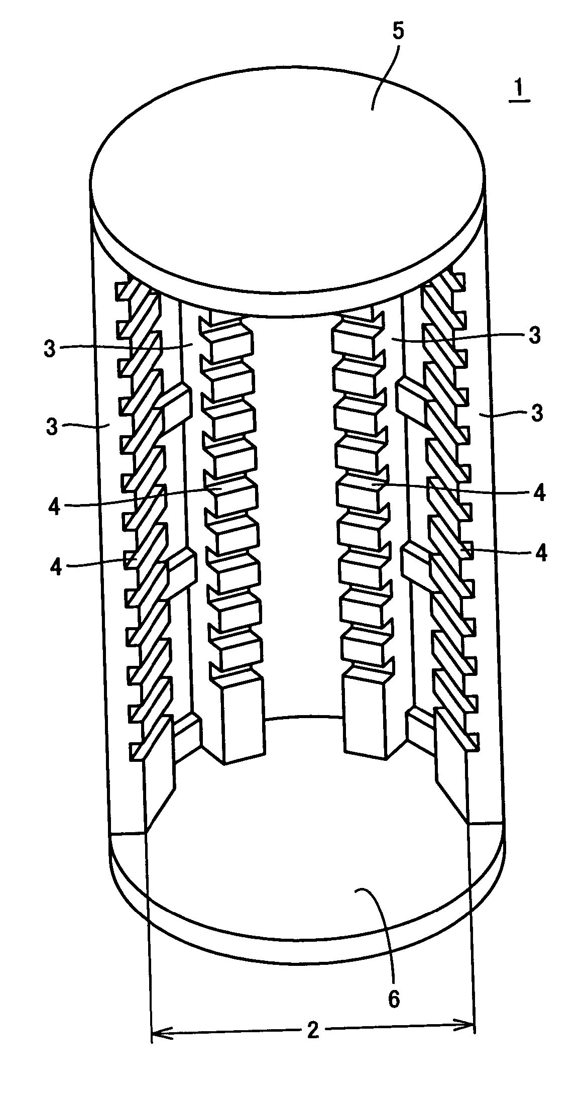
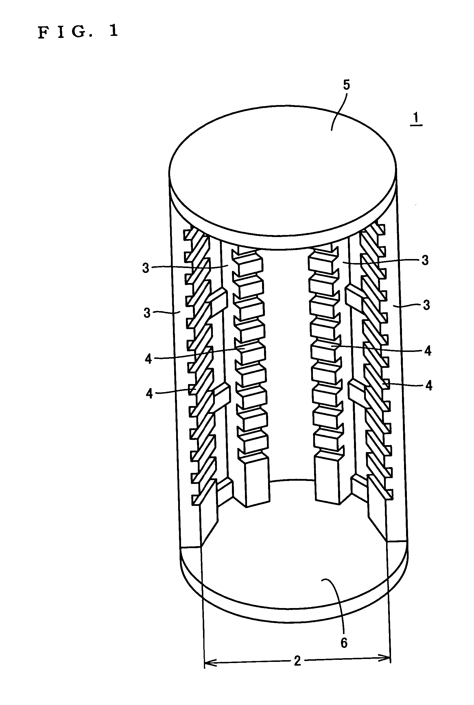
A heat treatment jig for supporting silicon semiconductor substrates by contacting, being loaded onto a heat treatment boat in a vertical heat treatment furnace, comprises; the configuration of a ring or a disc structure with the wall thickness between 1.5 and 6.0 mm; the deflection displacement of 100 μm or less at contact region in loaded condition; the outer diameter which is 65% or more of the diameter of said substrate; and the surface roughness (Ra) of between 1.0 and 100 μm at the contact region. The use of said jig enables to effectively retard the slip generation and to avoid the growth hindrance of thermally oxidized film at the back surface of said substrate, diminishing the surface steps causing the defocus in photolithography step in device fabrication process, thereby enabling to maintain high quality of silicon semiconductor substrates and to substantially enhance the device yield.

Description

BACKGROUND OF THE INVENTION [0001] 1. Field of the Invention [0002] The present invention relates to a heat treatment jig that is used in a heat treatment boat of a vertical heat treatment furnace, and in more detail, to a heat treatment jig for silicon semiconductor substrates that can retard the generation of slips as crystal defects during heat treatment at high temperature and can prevent the generation of surface steps attributable to the growth hindrance of the thermally oxidized film which generates at the back surface of said silicon semiconductor substrates when being held in oxidizing atmosphere in high temperature heat treatment. [0003] 2. Description of the Related Art [0004] A silicon semiconductor substrate that is processed in LSI device fabrication process, in fabrication steps such as oxidation, diffusion, film deposition and the like, is repeatedly subjected to high temperature heat treatment. [0005] In heat treatment of silicon semiconductor substrates, a vertical...

Claims


Application Information

Patent Timeline
IPC IPC(8): F27D5/00H01L21/22H01L21/31H01L21/324H01L21/673H01L21/68
CPCF27D5/0037H01L21/67303H01L21/67323H01L21/67309H01L21/6732H01L21/67306
Inventor ADACHI, NAOSHI
Owner SUMITOMO MITSUBISHI SILICON CORP
Learn More