Method and structure for manufacturing improved yield semiconductor packaged devices

a technology of packaged devices and semiconductors, applied in semiconductor devices, semiconductor/solid-state device details, electrical apparatus, etc., can solve problems such as thermal mismatch stress, failure to meet the requirements of the sealing process, so as to achieve high reliability and alleviate thermal mismatch stress

Inactive Publication Date: 2005-12-29
ROUND ROCK RES LLC
View PDF2 Cites 1 Cited by
  • Summary
  • Abstract
  • Description
  • Claims
  • Application Information

AI Technical Summary

Benefits of technology

[0012] The present invention is directed to a high reliability semiconductor package structure. The package structure is a ball grid array. type package that uses a plurality of pieces of adhesive film to attach a semiconductor die to a substrate having conductive traces in order to alleviate thermal mismatch stress between the semiconductor die and the printed circuit board to which the packaged device is soldered, while maintaining the reliability of the packaged device itself.

Problems solved by technology

However, there may be an issue with regards to the reliability of the solder joints as a result of the different expansion rates of the semiconductor die of the packaged device and the PCB to which the packaged device is soldered.
The thermal mismatch results in a shearing stress focused at the interface between the packaged device and the PCB, namely, the solder joints.
The reliability of the electronic system is compromised when the thermal mismatch stress applied to the solder joints of the packaged device is great enough to cause one of the solder joints to fail.
However, in the case where TAB wire connections are used in such a package structure to electrically couple the bond pads of the die to the conductive traces of the substrate, thermal expansion of the elastomer pad creates reliability problems for the packaged device itself.
It has been shown in reliability testing that the TAB wire joint is the point most susceptible to failure when the packaged device is subjected to temperature cycle tests (e.g., −65° C. to +150° C.) or high temperature and humidity tests (e.g., 85° C., 85% RH, alternating bias).
Consequently, the resulting compliant structure places stress at the TAB wire joint where the wire is bonded to the bond pad of the die.
Although the resulting compliant structure accommodates the different expansion rates of the die and the PCB, the assembly process is time-consuming.
Variations in the screen printing process or in the attachment of dry adhesive to the elastomer posts may result in unacceptable coplanarity, and consequently, unacceptable packaged devices.

Method used


Image

  • Method and structure for manufacturing improved yield semiconductor packaged devices
  • Method and structure for manufacturing improved yield semiconductor packaged devices
  • Method and structure for manufacturing improved yield semiconductor packaged devices

Examples


Embodiment Construction

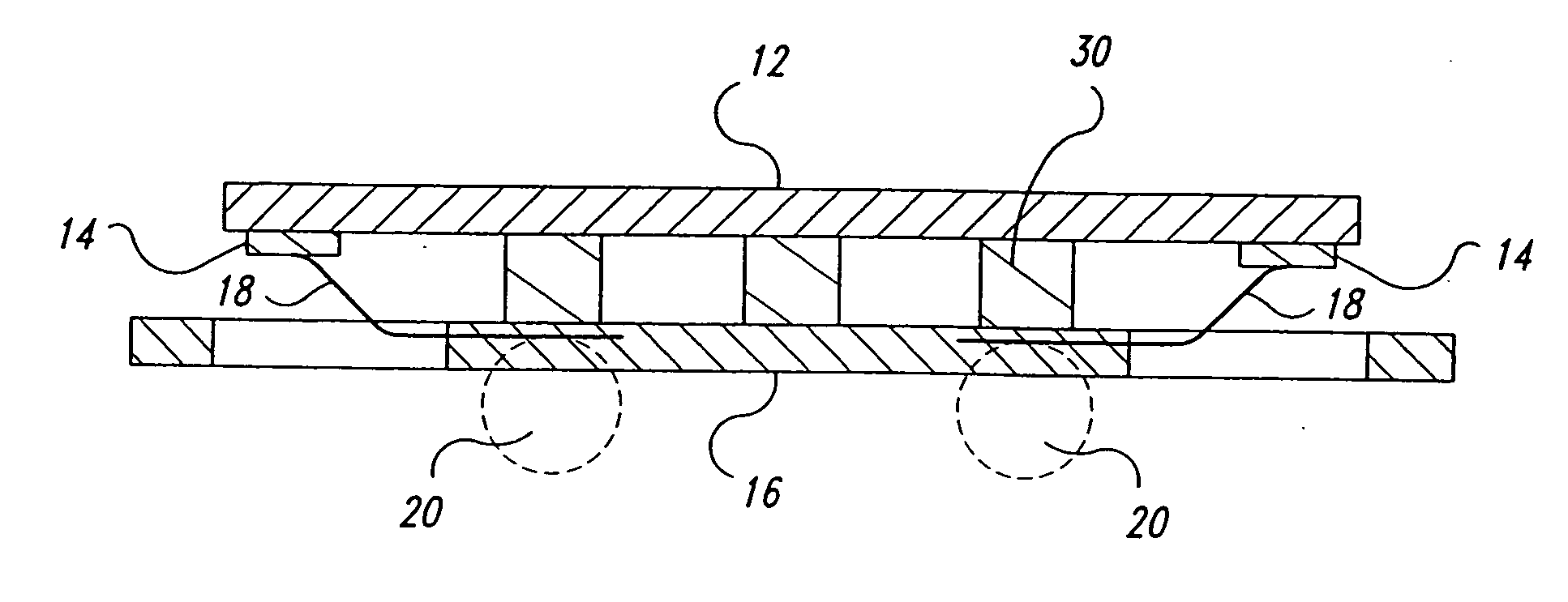
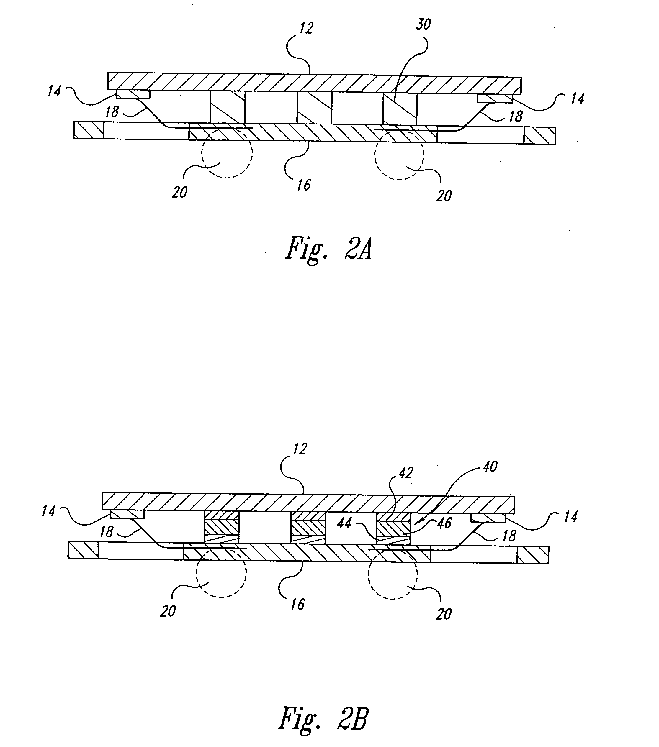
[0016] Embodiments of the present invention use a plurality of pieces of adhesive film to attach a semiconductor die to a substrate in a BGA type package. Using multiple pieces of adhesive film alleviates some of the thermal mismatch stress between the semiconductor die and the PCB to which the packaged device is soldered, while maintaining the reliability of the packaged device itself. As will be illustrated below, the sum change in the length of the pieces of adhesive film will be less than the change in the length of a elastomer pad of a conventional BGA package structure of similar size. Thus, the stress applied to the TAB wire joints caused by thermal expansion will be reduced with respect to the conventional package structure. The pieces of adhesive film are attached to the substrate by pressure bonding, and the die is subsequently pressure bonded to the opposite surface of the pieces of adhesive film. Coplanarity of the die and the substrate is maintained by the substantially...


PUM


Abstract

A semiconductor package structure for a ball grid array type package using a plurality of pieces of adhesive elastomer film to attach a semiconductor die to a substrate having conductive traces in order to alleviate thermal mismatch stress between the semiconductor die and the printed circuit board to which the packaged device is soldered, while maintaining the reliability of the packaged device itself.

Description

TECHNICAL FIELD [0001] The present invention relates to semiconductor packaging, and more particularly, to attaching a semiconductor die in a device package. BACKGROUND OF THE INVENTION [0002] Semiconductor devices are typically fabricated on thin wafers of silicon. Several dice are produced on each wafer, with each die representing a single semiconductor device. Each die on a wafer is tested for gross functionality, and sorted according to whether the die passes or fails the gross functionality test. After being sorted according to gross functionality, the wafers are cut using a wafer saw, and the individual die are singulated. The die determined to be non-functional are scrapped. The functional die are packaged and further tested to ensure that each packaged device satisfies a minimum level of performance. Typically, the functional devices are permanently packaged by encapsulating the die in a plastic package. Packaging of the functional devices facilitates handling of the devices...

Claims


Application Information

Patent Timeline
Patent Type & Authority Applications(United States)
IPC IPC(8): H01L23/12H01L21/44H01L21/58H01L21/60H01L23/48H01L23/498
CPCH01L23/49827H01L2224/0401H01L24/16H01L24/48H01L24/73H01L24/81H01L24/83H01L2224/05599H01L2224/13099H01L2224/32014H01L2224/48H01L2224/83194H01L2224/8385H01L2224/85399H01L2924/01005H01L2924/01006H01L2924/01013H01L2924/01014H01L2924/01082H01L2924/014H01L2924/07802H01L2924/14H01L2924/15311H01L24/32H01L2924/00014H01L2924/01033H01L2924/01045H01L2924/01087H01L24/11H01L2224/81903H01L2224/81192H01L2224/73203H01L2224/2919H01L2224/29013H01L2224/16237H01L2224/81136H01L2224/30131H01L2224/29036H01L2224/45099H01L2224/50H01L21/60
Inventor JIANG, TONGBI
Owner ROUND ROCK RES LLC
Why Eureka
Try Eureka