Electric non-polarized composite gallium nitride base substrate and production method
- Summary
- Abstract
- Description
- Claims
- Application Information
AI Technical Summary
Problems solved by technology
Method used
Image

Examples
example
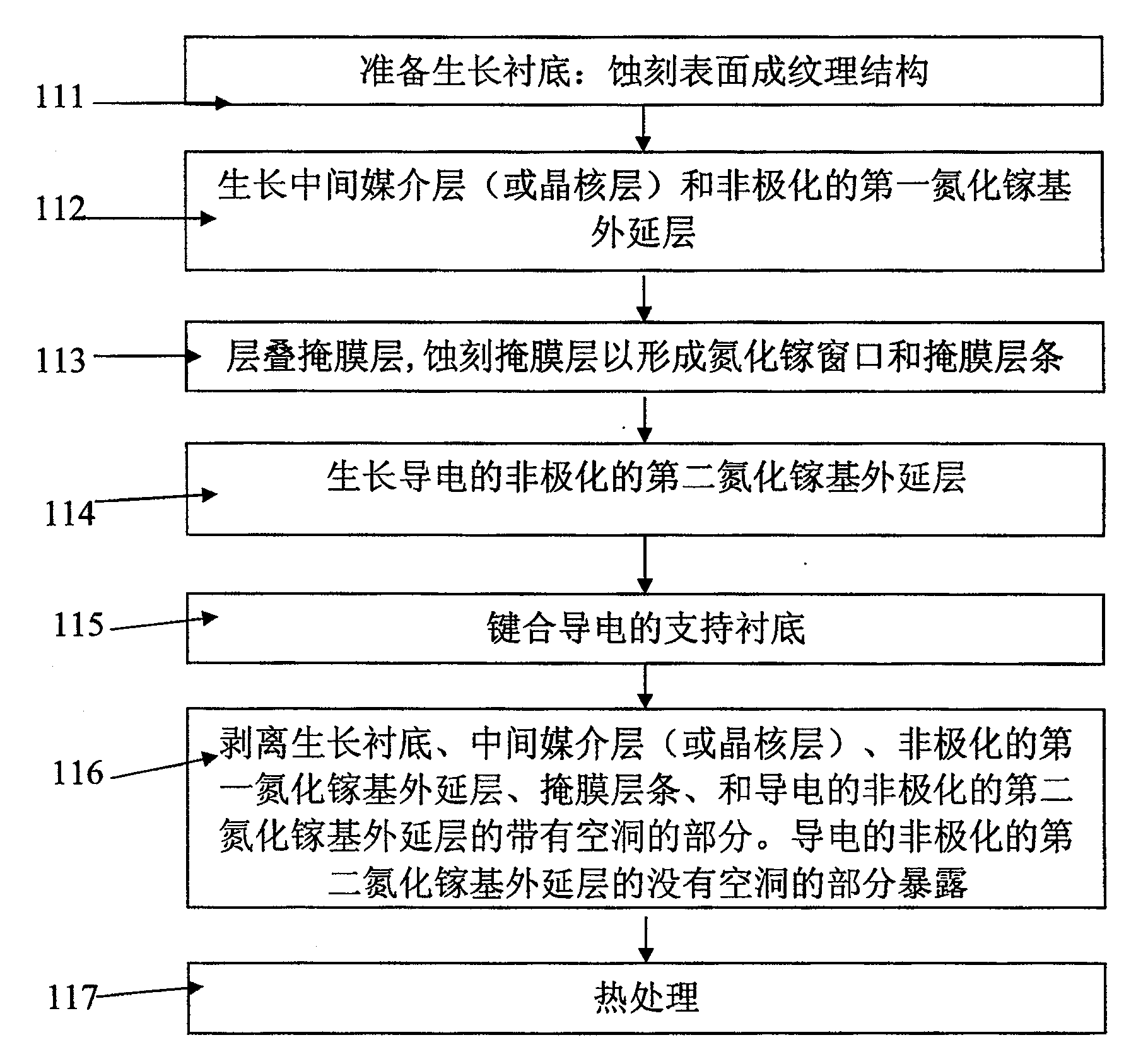
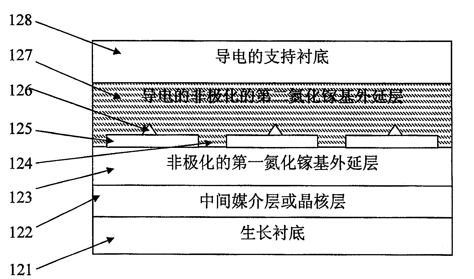
[0047] The first specific implementation example of the process flow step 112: using MOCVD, grow a layer of gallium nitride substrate with a thickness between 1 nm and 90 nm on the r-plane sapphire growth substrate (at a temperature of 400-900 ° C). Nucleation layer. The material of the crystal nucleus layer includes, but is not limited to, gallium nitride. An a-plane non-polarized first GaN-based epitaxial layer is grown on the crystal nucleus layer. A specific implementation example of growing a non-polarized a-plane first gallium nitride-based epitaxial layer: growing a non-polarized a-plane at a temperature above about 1000° C. and at a pressure less than 1 atmosphere, with an appropriate V / III ratio The thickness of the first GaN-based epitaxial layer is 1-5 microns.
[0048] A second specific implementation example of process flow step 112: using MBE, grow an aluminum nitride buffer layer on an m-plane 6H-silicon carbide growth substrate, and then grow an m-plane first...
PUM
| Property | Measurement | Unit |
|---|---|---|
| thickness | aaaaa | aaaaa |
| thickness | aaaaa | aaaaa |
| size | aaaaa | aaaaa |
Abstract
Description
Claims
Application Information