Analog-to-digital converter and method of analog-to-digital conversion

Active Publication Date: 2005-12-29
DENSO CORP
View PDF6 Cites 9 Cited by
  • Summary
  • Abstract
  • Description
  • Claims
  • Application Information

AI Technical Summary

Benefits of technology

[0031] By dividing the A/D-converted data set of the voltage signal by the A/D-converted data set of the reference voltage, any variation of the A/D-converted data set of the voltage signal due to variations of the delay times of the delay gates constituting the pulse-circulating circuit can be eliminated.
[0032] Since the A/D converted data set of the reference voltage is stored

Problems solved by technology

However, converting an analog voltage signal into corresponding digital data by use of such a PPDC circuit 1 involves a problem in that the binary digital data set D01 varies as ambient temperature varies, because the inverting time of each of the NAND gate 2b and the inverting gates 2a is temperature-dependent.
However, there arises a problem in a case where the reference voltage VR is

Method used


Image

  • Analog-to-digital converter and method of analog-to-digital conversion
  • Analog-to-digital converter and method of analog-to-digital conversion
  • Analog-to-digital converter and method of analog-to-digital conversion

Examples


first embodiment

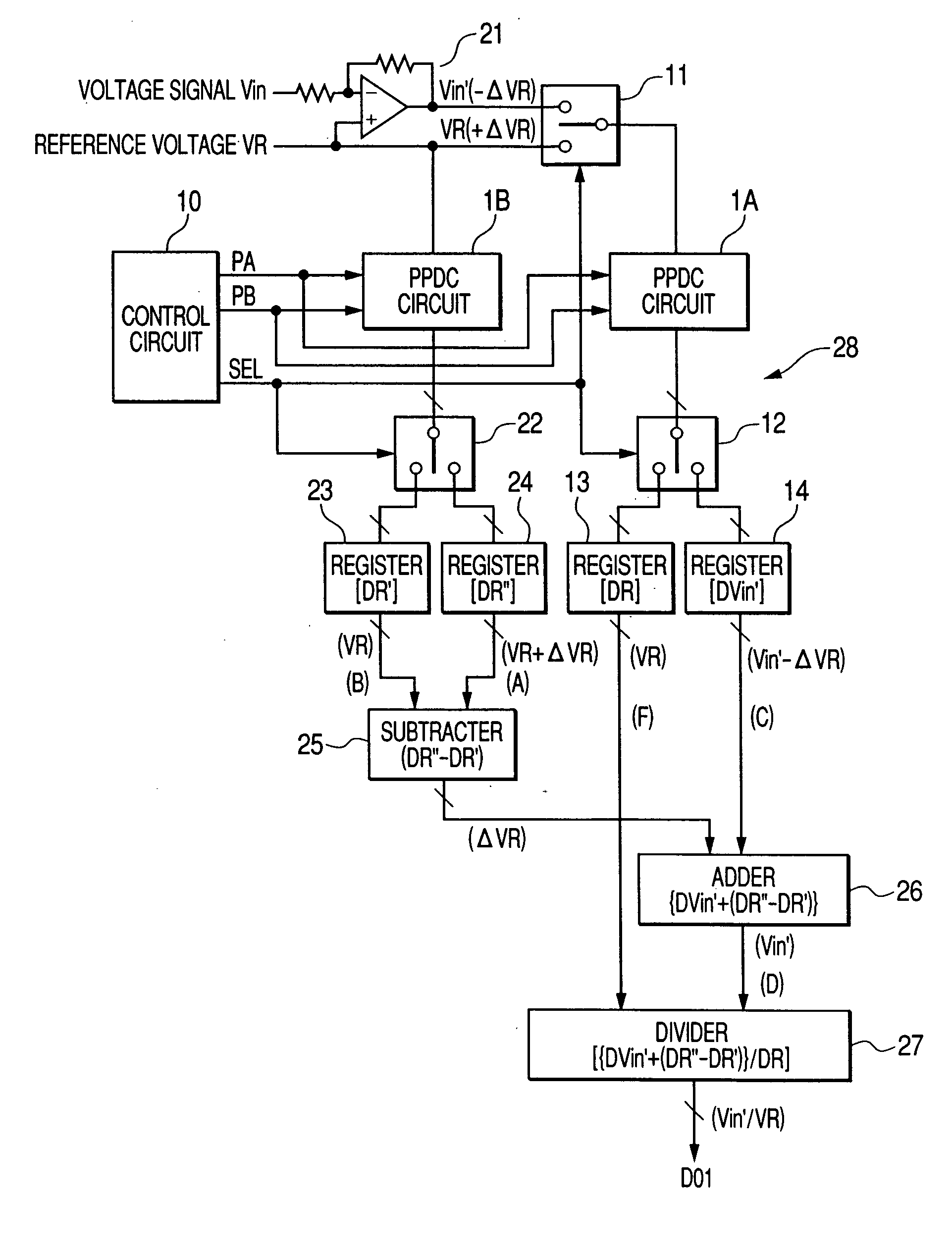
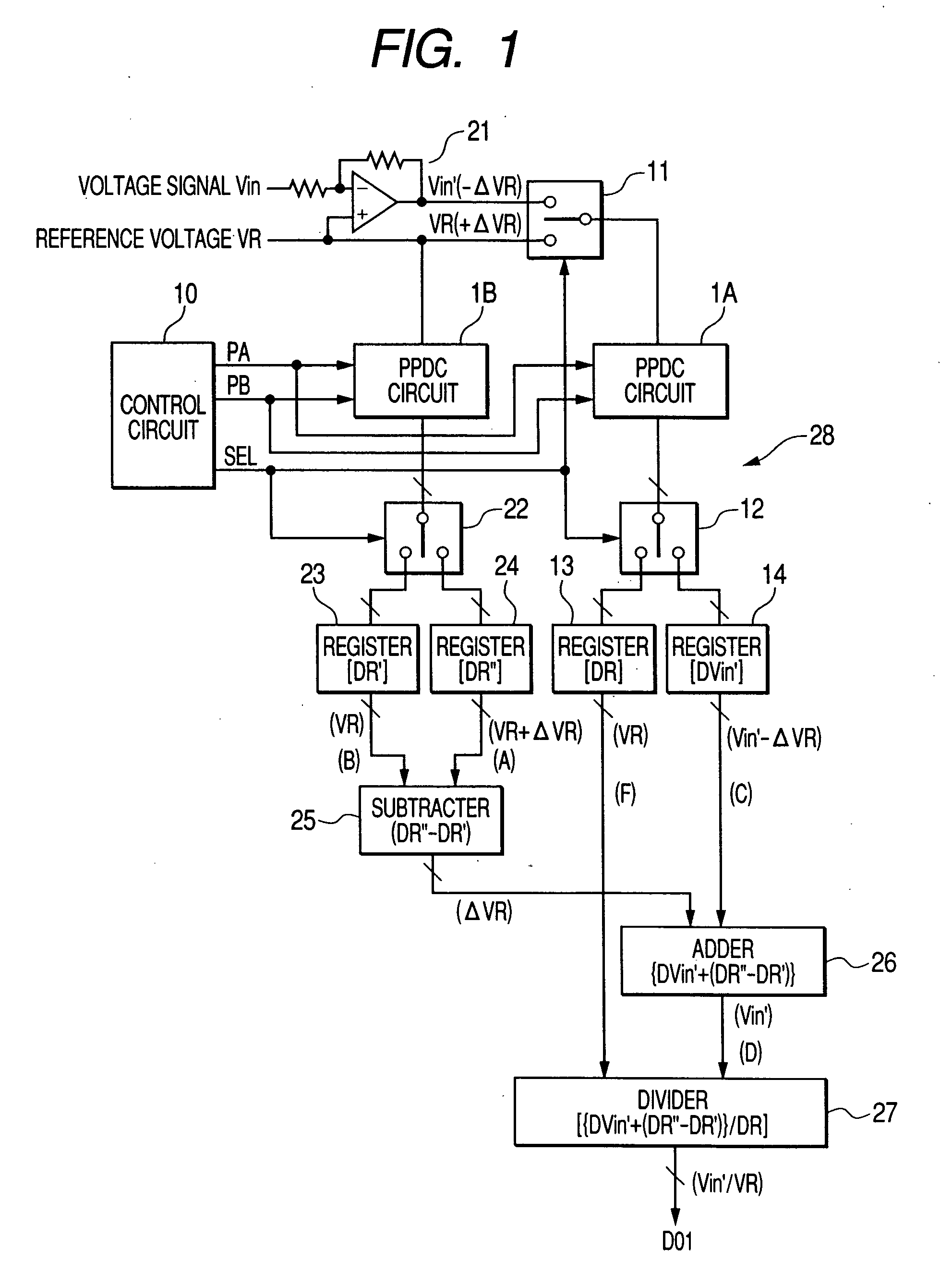
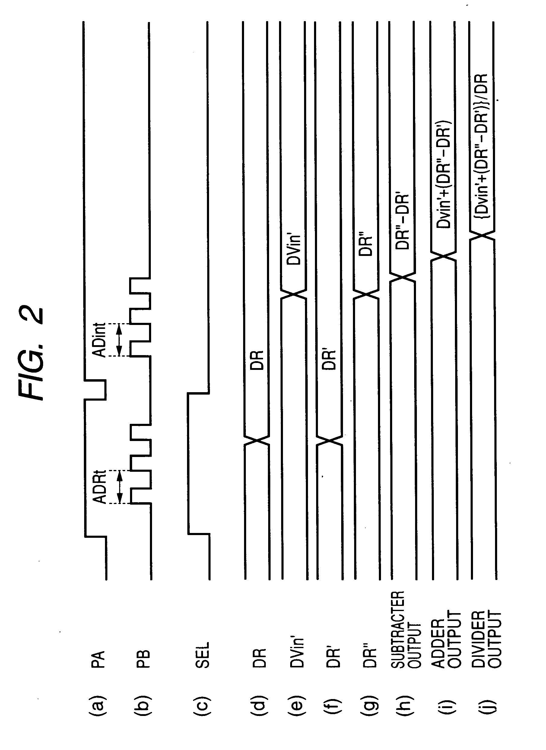
[0056]FIG. 1 is a block diagram showing a structure of an A / D converter according to a first embodiment of the invention. As shown in FIG. 1, this A / D converter 28 includes a PPDC (Pulse-Phase-Difference Coding) circuit 1A, a PPDC circuit 1B, a control circuit 10, an inverting amplifier 21, an input-selection switch 11, output selection switches 12, 22, registers 13, 14, 23, 24, a subtracter 25, an adder 26, and a divider 27. The PPDC circuits 1A and 1B have the same structure and operate in a like manner as the PPDC circuit 1 shown in FIG. 19.

[0057] The analog voltage signal Vin is amplified by the inverting amplifier 21 and then outputted to the input selection switch 11 as an analog voltage signal Vin′. The gain of the inverting amplifier 21 is one. The input selection switch 11 selects one of the analog voltage signal Vin′ and the reference voltage VR in accordance with a selection signal SEL received from the control circuit 10, and supplies it to the PPDC circuit 1A, The refe...

second embodiment

[0070]FIG. 4 is a block diagram showing a structure of an A / D converter 33 according to a second embodiment of the invention. In FIG. 4, elements that are the same as those shown in FIG. 1 are given the same reference characters, and explanation thereof will be omitted. The second embodiment is different from the first embodiment in that the second embodiment uses a non-inverting amplifier 31 and a subtracter 32 (variation compensation circuit) instead of the inverting amplifier 21 and the adder 26.

[0071] The operation of the A / D converter 33 according to the second embodiment of the invention is explained below. Assume that the reference voltage VR has increased larger by +ΔVR since the time when the PPDC circuit 1A performed A / D conversion on the reference voltage VR, so that the value of the analog voltage signal Vin′ presently received by the PPDC circuit 1A is represented by (Vin+ΔVR) (see FIG. 5).

[0072] In this case, the subtracter 32 outputs, as a subtraction result, a data...

third embodiment

[0073]FIG. 6 is a block diagram showing a structure of an A / D converter 35 according to a third embodiment of the invention. The third embodiment is different from the first embodiment in that the registers 14, 24 are eliminated, and the subtracter 25 and the adder 26 are replaced by a subtraction / addition device (variation compensation circuit) 34.

[0074] In the third embodiment, the data set DR and the data set DR′ A / D-converted by the PPDC circuit 1A and the PPDC circuit 1B, respectively, are stored in the register 13 and 23, respectively, as with the case of the first embodiment. However, the data set representing the value of (Vin′−ΔVR) A / D-converted by the PPDC circuit 1A, and the data set representing the value of (VR) or (VR+ΔVR) A / D-converted by the PPDC circuit 1B are directly sent to the subtraction / addition device 34. Accordingly, the third embodiment can be made simpler than the first embodiment in structure.


PUM


Abstract

The A/D converter has first and second PPDC circuits (pulse-phase-difference coding circuits). The first PPDC circuit performs A/D conversions on the reference voltage and on the voltage signal amplified by an amplifier in an alternating sequence, the amplifier using the reference voltage as a potential base thereof. The second PPDC circuit performs A/D conversions always on the reference voltage. The A/D-converted data set of the voltage signal outputted from the first PPDC circuit is corrected depending on the difference between the A/D-converted data set of the reference voltage outputted from the second PPDC circuit when the first PPDC circuit A/D-converts the reference voltage and the A/D-converted data set of the reference voltage outputted from the second PPDC circuit when the first PPDC circuit A/D-converts the voltage signal.

Description

CROSS-REFERENCE TO RELATED APPLICATION [0001] This application is related to Japanese Patent Applications No. 2004-31945 filed on Feb. 9, 2004, and No. 2004-34909 filed on Feb. 12, 2004, the contents of which are hereby incorporated by reference. BACKGROUND OF THE INVENTION [0002] 1. Field of the Invention [0003] The present invention relates to an A / D (analog-to-digital) converter and an A / D conversion method for converting an analog voltage signal into digital data. [0004] 2. Description of Related Art [0005] As disclosed in Japanese Patent Application Laid-open No. 5-259907, it is known to convert an analog voltage signal into a digital signal by use of a pulse-phase-difference coding circuit. It is also known to use the pulse-phase-difference coding circuit as a filter for removing high frequency noises included in an input analog voltage signal as disclosed in Japanese Patent Application Laid-open No. 2002-217758. [0006]FIG. 19 shows a structure of such a pulse-phase-difference...

Claims


Application Information

Patent Timeline
IPC IPC(8): H03M1/12H03M1/64
CPCH03M1/64
Inventor HARADA, TAKUYAHORIE, MASAKIYOHONDA, TAKUYATANAKA, NOBUYUKI
Owner DENSO CORP
Why Eureka
Try Eureka