Output Current Monitor Circuit for Switching Regulator
a current monitor and switching regulator technology, applied in the direction of electric variable regulation, pulse manipulation, instruments, etc., can solve the problems of sensing error, power consumption is also a key design requirement, etc., and achieve the effect of minimal power consumption
- Summary
- Abstract
- Description
- Claims
- Application Information
AI Technical Summary
Benefits of technology
Problems solved by technology
Method used
Image
Examples
first embodiment
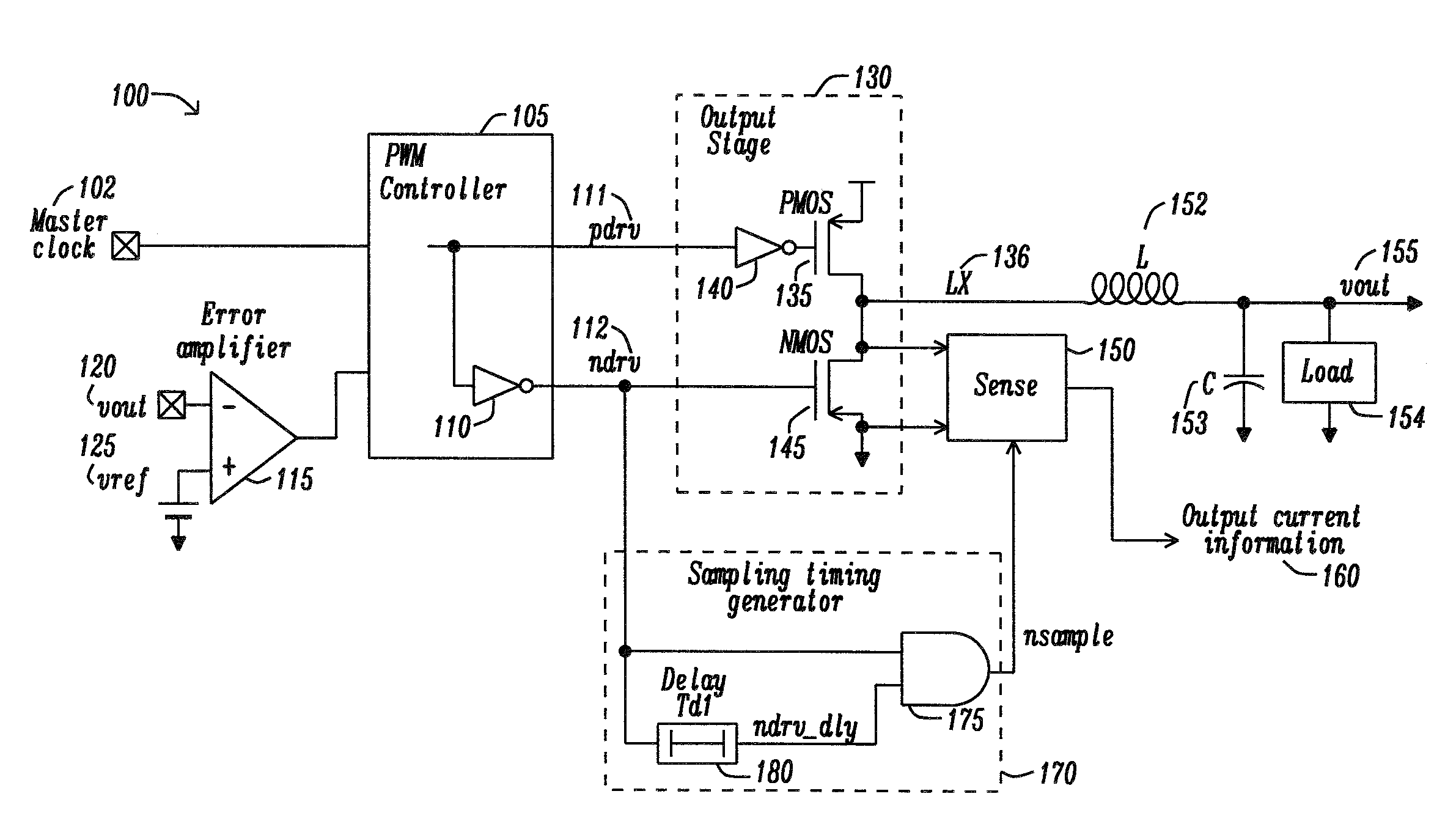
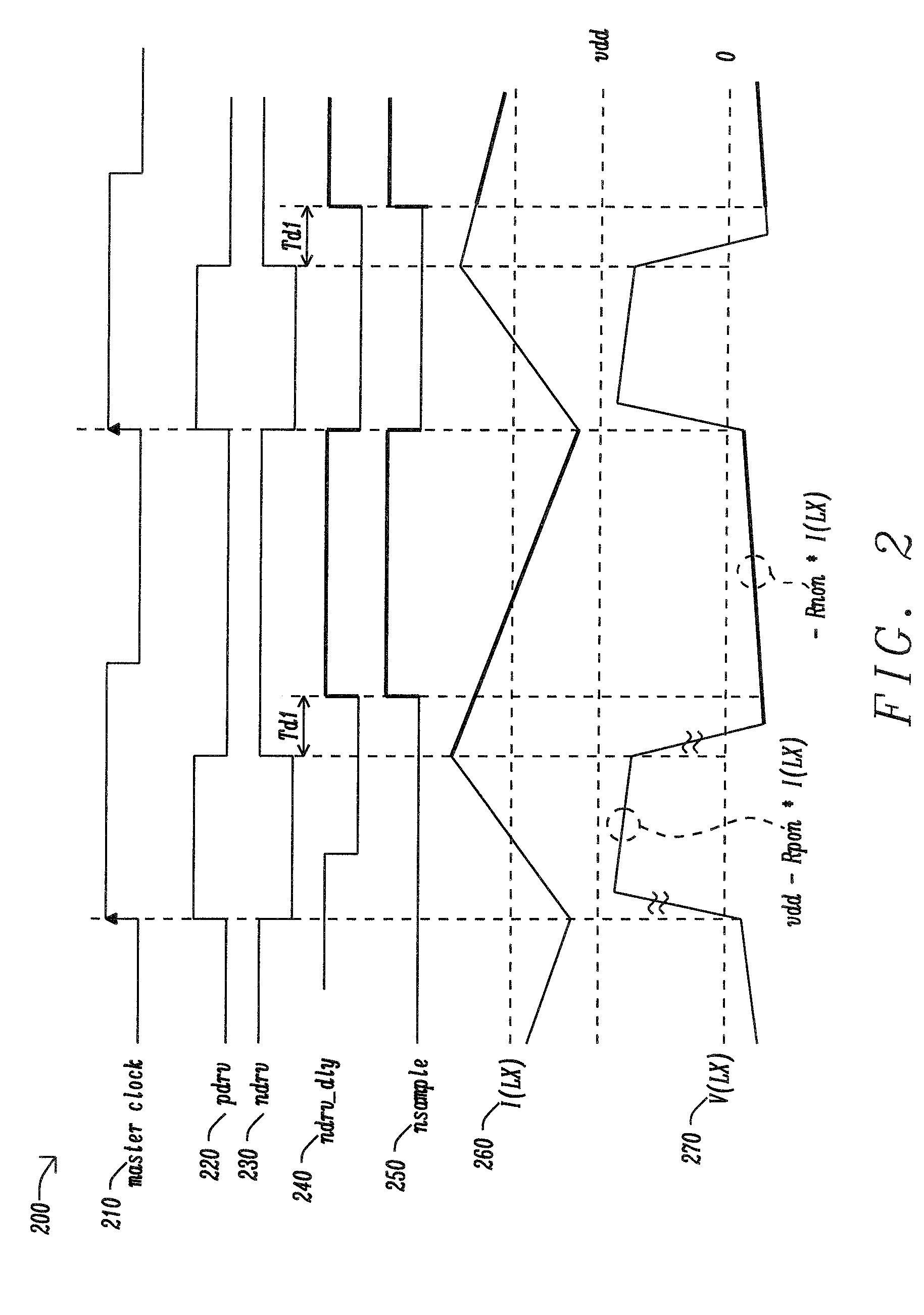
[0038]FIG. 3 is a circuit schematic in accordance with the disclosure. FIG. 3 shows a block diagram of the invention. The Master clock 302 is delayed by the delay element Delay Td2303 and used for PWM controller 305. Sampling signal nsample is generated in the Sampling timing generator 370. It starts the first delay element Delay Td1377 after ndrv is activated. Its end is the second delay element Delay Td2303 earlier than ndrv, because nsample is reset by Master clock 302 but signal ndrv 312 is reset by delayed clock. This sampling timing generator is logic circuit and various kinds of implementations are possible. The necessary elements are as follows: (1) the first flip-flop which is set by rise of master clock and reset when sampling signal is inactive; (2) the second flip-flop of which output is sampling signal which is set by delayed ndrv, and reset when ndrv is inactive or when first flip-flop is active, (3) and a delay which is generated delayed ndrv from ndrv.
[0039]FIG. 3 sh...
second embodiment
[0045]FIG. 5 is a circuit schematic in accordance with the disclosure. FIG. 5 shows average output current monitor implemented in a buck regulator. The essential elements in this implementation for the sampling timing generator are: (1) Sampling timing is generated as AND of ndrv, ndrv_dly and mask signal; (2) Ndrv_dly is delay of ndrv, and (3) a mask signal is inactive only from master clock's rise to delayed clock's rise. The buck 500 is composed of PWM controller 505 and output stage 530. Output current monitor is sampling timing generator 570, sampler and sense circuit 550. The PWM controller 505 has an input signal from Master clock signal 502, followed by the second delay element Delay Td2503, and a second input signal from Error amplifier 515. The Error amplifier 515 has two inputs, with a vout signal 520 and reference signal vref 525. The PWM controller 505 generates two output signals pdrv 511 and ndrv 512. The Output stage 530 contains PMOS 535 and pre-drive inverter 540, ...
PUM
 Abstract
Description
Claims
Application Information


