Flash EEprom system

a flash eeprom and chip technology, applied in the field of integrated circuit flash eeprom chips, can solve the problems of reliability problems, disadvantages of disk drives, and requirement for high-precision moving mechanical parts

Inactive Publication Date: 2005-12-29
SANDISK TECH LLC
View PDF76 Cites 49 Cited by
  • Summary
  • Abstract
  • Description
  • Claims
  • Application Information

AI Technical Summary

Benefits of technology

[0016] According to yet another aspect of the present invention, a write cache is used to minimize the number of writes to the Flash EEprom memory. In this way the Flash EEprom memory will be subject to fewer stress inducing write / erase cycles, thereby retarding its aging. The most active data files are written to the cache memory instead of the Flash EEprom memory. Only when the activity levels have reduced to a predetermined level are the data files written from the cache memory to the Flash EEprom memory. Another advantage of the invention is the increase in write throughput by virtue of the faster cache memory.
[0017] According to yet another aspect of the present invention, one or more printed circuit cards are provided which contain controller and EEprom circuit chips for use in a computer system memory for long term, non-volatile storage, in place of a hard disk system, and which incorporate various of the other aspects of this invention alone and in combination.

Problems solved by technology

However, disk drives are disadvantageous in that they are bulky and in their requirement for high precision moving mechanical parts.
Consequently they are not rugged and are prone to reliability problems, as well as consuming significant amounts of power.
However, they are much more expensive, and require constant power to maintain their memory (volatile).
Moreover, they are nonvolatile, and retain their memory even after power is shut down.
However, conventional Flash EEprom's have a limited lifetime in terms of the number of write (or program) / erase cycles they can endure.
Typically the devices are rendered unreliable after 102 to 103 write / erase cycles.

Method used


Image

  • Flash EEprom system
  • Flash EEprom system
  • Flash EEprom system

Examples


Embodiment Construction

EEprom System

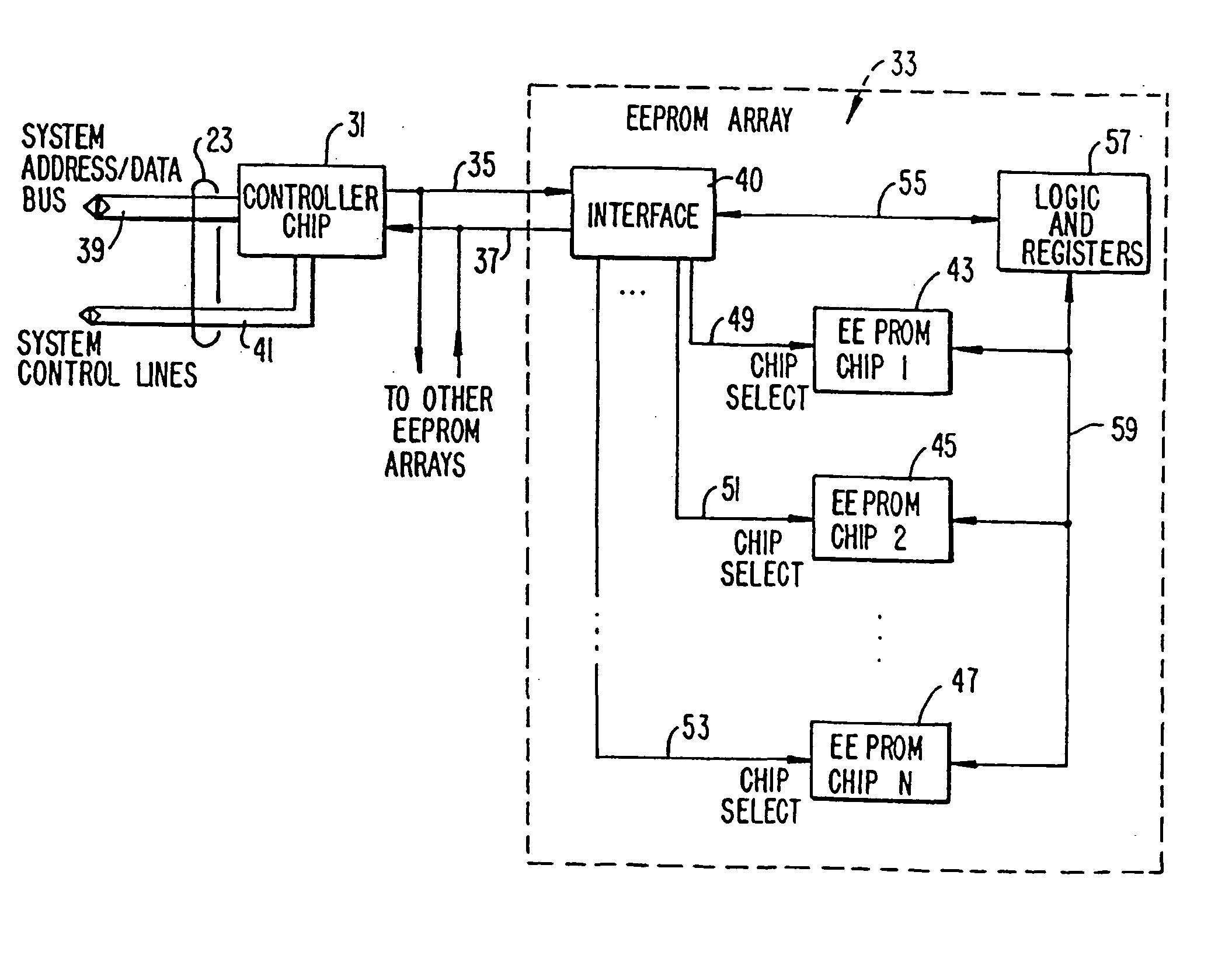
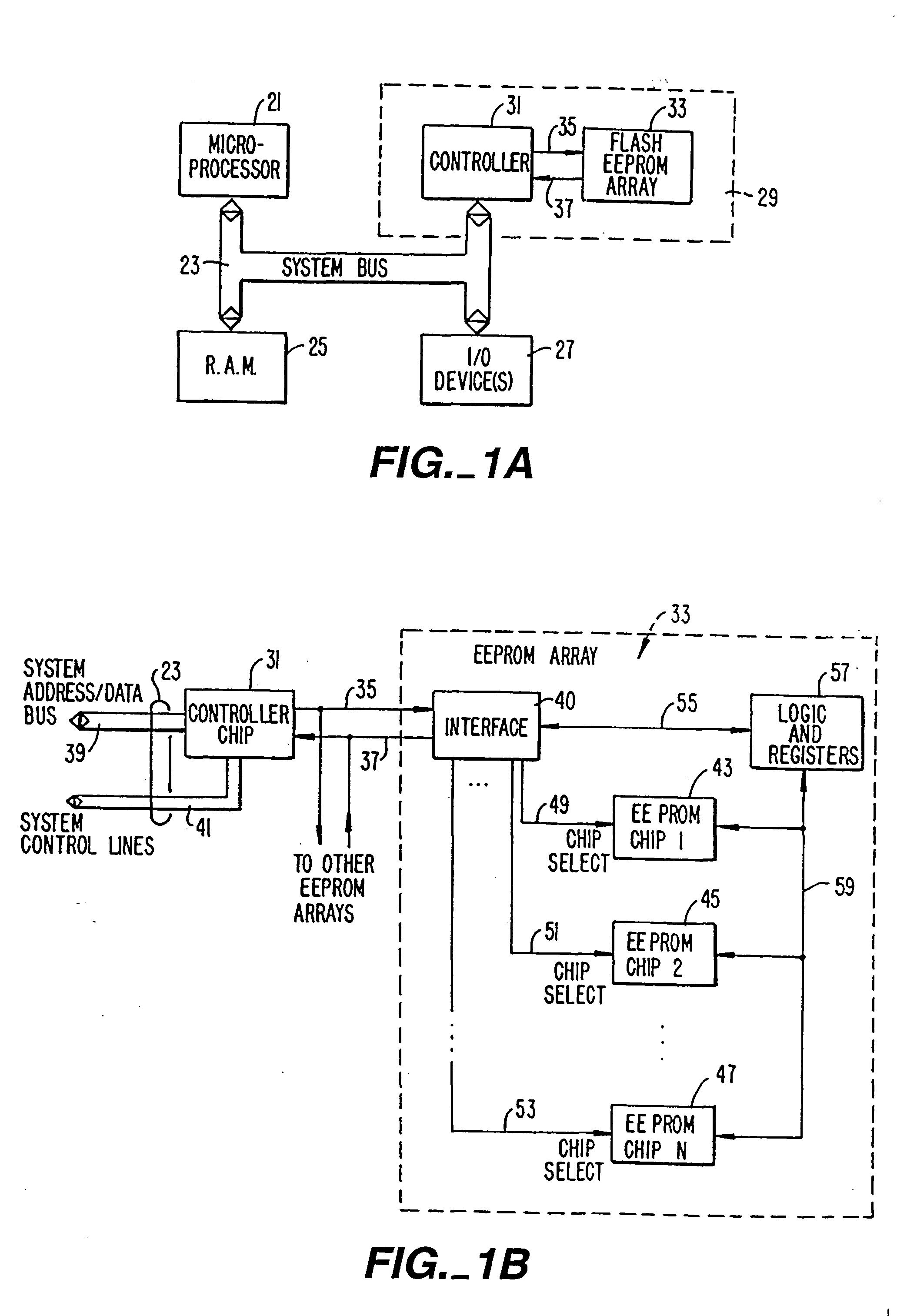
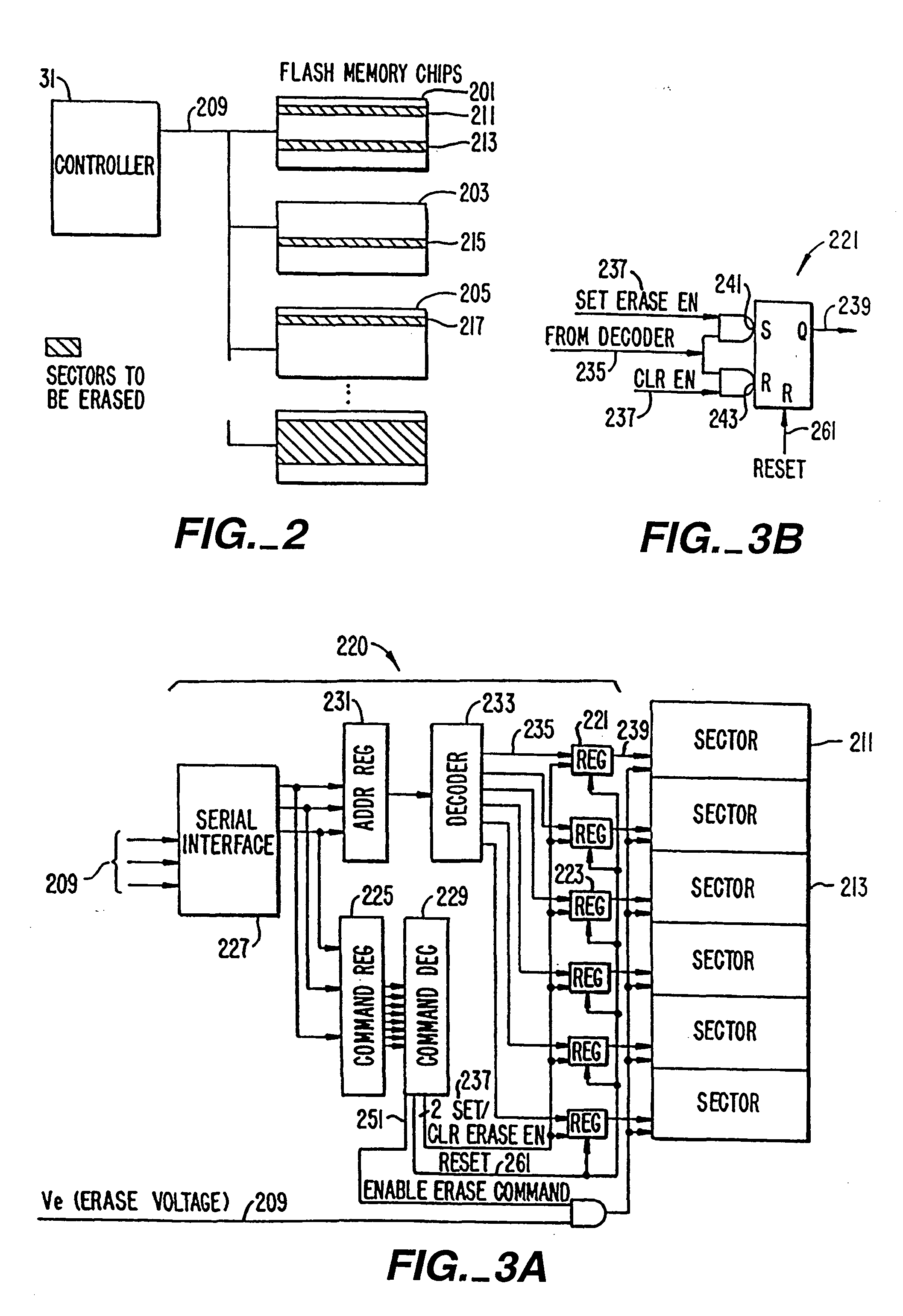
[0029] A computer system in which the various aspects of the present invention are incorporated is illustrated generally in FIG. 1A. A typical computer system architecture includes a microprocessor 21 connected to a system bus 23, along with random access, main system memory 25, and at least one or more input-output devices 27, such as a keyboard, monitor, modem, and the like. Another main computer system component that is connected to a typical computer system bus 23 is a large amount of long-term, non-volatile memory 29. Typically, such a memory is a disk drive with a capacity of tens of megabytes of data storage. This data is retrieved into the system volatile memory 25 for use in current processing, and can be easily supplemented, changed or altered.

[0030] One aspect of the present invention is the substitution of a specific type of semiconductor memory system for the disk drive but without having to sacrifice non-volatility, ease of erasing and rewriting data in...


PUM


Abstract

A system of Flash EEprom memory chips with controlling circuits serves as non-volatile memory such as that provided by magnetic disk drives. Improvements include selective multiple sector erase, in which any combinations of Flash sectors may be erased together. Selective sectors among the selected combination may also be de-selected during the erase operation. Another improvement is the ability to remap and replace defective cells with substitute cells. The remapping is performed automatically as soon as a defective cell is detected. When the number of defects in a Flash sector becomes large, the whole sector is remapped. Yet another improvement is the use of a write cache to reduce the number of writes to the Flash EEprom memory, thereby minimizing the stress to the device from undergoing too many write / erase cycling.

Description

BACKGROUND OF THE INVENTION [0001] This invention relates generally to semiconductor electrically erasable programmable read only memories (EEprom), and specifically to a system of integrated circuit Flash EEprom chips. [0002] Computer systems typically use magnetic disk drives for mass storage of data. However, disk drives are disadvantageous in that they are bulky and in their requirement for high precision moving mechanical parts. Consequently they are not rugged and are prone to reliability problems, as well as consuming significant amounts of power. Solid state memory devices such as DRAM's and SRAM's do not suffer from these disadvantages. However, they are much more expensive, and require constant power to maintain their memory (volatile). Consequently, they are typically used as temporary storage. [0003] EEprom's and Flash EEprom's are also solid state memory devices. Moreover, they are nonvolatile, and retain their memory even after power is shut down. However, conventional...

Claims


Application Information

Patent Timeline
Patent Type & Authority Applications(United States)
IPC IPC(8): G11C16/02G06F3/06G06F11/10G06F12/00G06F12/02G06F12/08G06F12/12G06F12/16G11C5/00G11C8/02G11C8/12G11C11/56G11C16/06G11C16/10G11C16/16G11C16/34G11C17/00G11C29/00G11C29/04G11C29/26G11C29/34G11C29/52H01L21/82H01L21/8247H01L27/115H01L29/788H01L29/792
CPCG06F3/0601G11C2216/18G06F3/064G06F3/0652G06F3/0679G06F3/068G06F3/0688G06F11/1068G06F12/0246G06F12/0802G06F12/0804G06F12/0866G06F12/0875G06F12/123G06F2003/0694G06F2212/2022G06F2212/312G06F2212/7201G06F2212/7203G06F2212/7205G06F2212/7207G06F2212/7208G11C7/1039G11C8/12G11C11/5621G11C11/5628G11C11/5635G11C16/10G11C16/16G11C16/3436G11C16/344G11C16/3445G11C16/3454G11C16/3459G11C29/00G11C29/26G11C29/34G11C29/52G11C29/765G11C29/82G11C2211/5621G11C2211/5634G11C2211/5643G06F3/0616G06F3/0664
Inventor HARARI, ELIYAHOUNORMAN, ROBERT D.MEHROTRA, SANJAY
Owner SANDISK TECH LLC
Why Eureka
Try Eureka