System and method for an asynchronous data buffer having buffer write and read pointers

a buffer and write pointer technology, applied in the memory system field, can solve the problems of reducing the hardware limitation of the memory device itself, affecting the performance of the memory device, and not related to the bandwidth limitation, so as to reduce the hardware limitation, the memory is typically more expensive, power and/or siz

Active Publication Date: 2005-12-29
MICRON TECH INC
View PDF99 Cites 59 Cited by
  • Summary
  • Abstract
  • Description
  • Claims
  • Application Information

AI Technical Summary

Problems solved by technology

Generally, bandwidth limitations are not related to the memory controllers since the memory controllers sequence data to and from the system memory as fast as the memory devices allow.
One reason for the non-linear relationship between data bus speed and bandwidth is the hardware limitations within the memory devices themselves.
Although these hardware limitations can be reduced to some degree through the design of the memory device, a compromise must be made because reducing the hardware limitations typically adds cost, power, and/or size to the memory devices, all of which are undesirable alternatives.
Thus, given these constraints, although it is easy for memory devices to move “well-behaved” traffic at ever increasing rates, for example, sequel traffic to the same page of a memory device, it is much more difficult for the memory devices to resolve “badly-behaved traffic,” such as bouncing between different pages or banks of the memory device.
As a result, the increase in memory data bus bandwidth does not always yield a corresponding increase in information bandwidth.
In addition to the limited bandwidth between processors and memory devices, the performance of computer systems is also limited by latency problems that increase the time required to read data from system memory devices.
Therefore, although SDRAM devices can synchronously output burst data at a high data rate, the delay in initially providing the data can significantly slow the operating speed of a computer system using such SDRAM devices.
However, as with bandwidth, the increase in memory data bus speeds do not yield a linear reduction of latency, f

Method used


Image

  • System and method for an asynchronous data buffer having buffer write and read pointers
  • System and method for an asynchronous data buffer having buffer write and read pointers
  • System and method for an asynchronous data buffer having buffer write and read pointers

Examples


Embodiment Construction

[0021] Embodiments of the present invention are directed to a read data synchronization circuit for coupling read data across two clock domains and providing information on the timing margin between when read data is made available and when the data can be retrieved. Certain details are set forth below to provide a sufficient understanding of various embodiments of the invention. However, it will be clear to one skilled in the art that the invention may be practiced without these particular details. In other instances, well-known circuits, control signals, and timing protocols have not been shown in detail in order to avoid unnecessarily obscuring the invention.

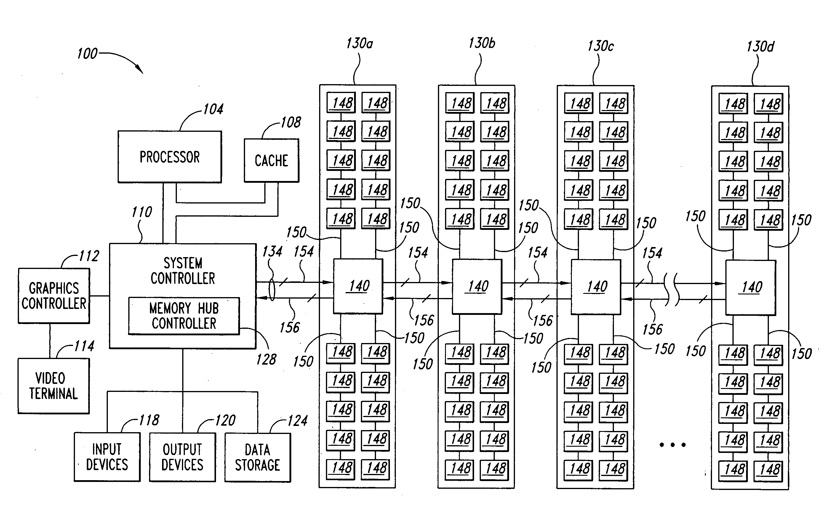
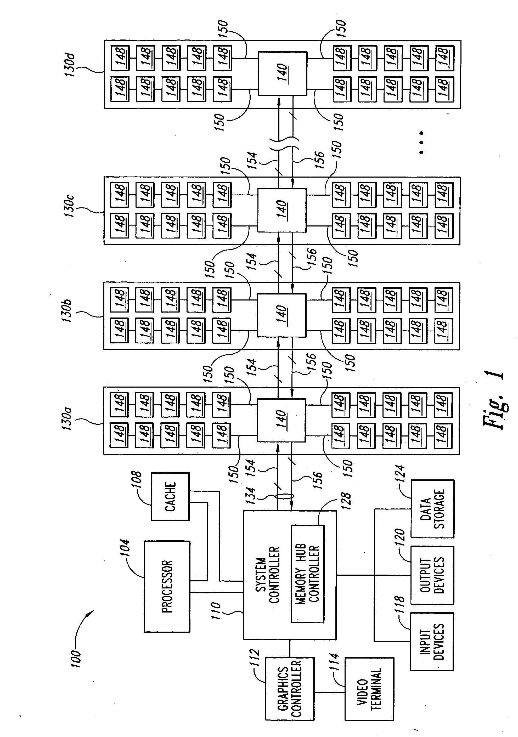
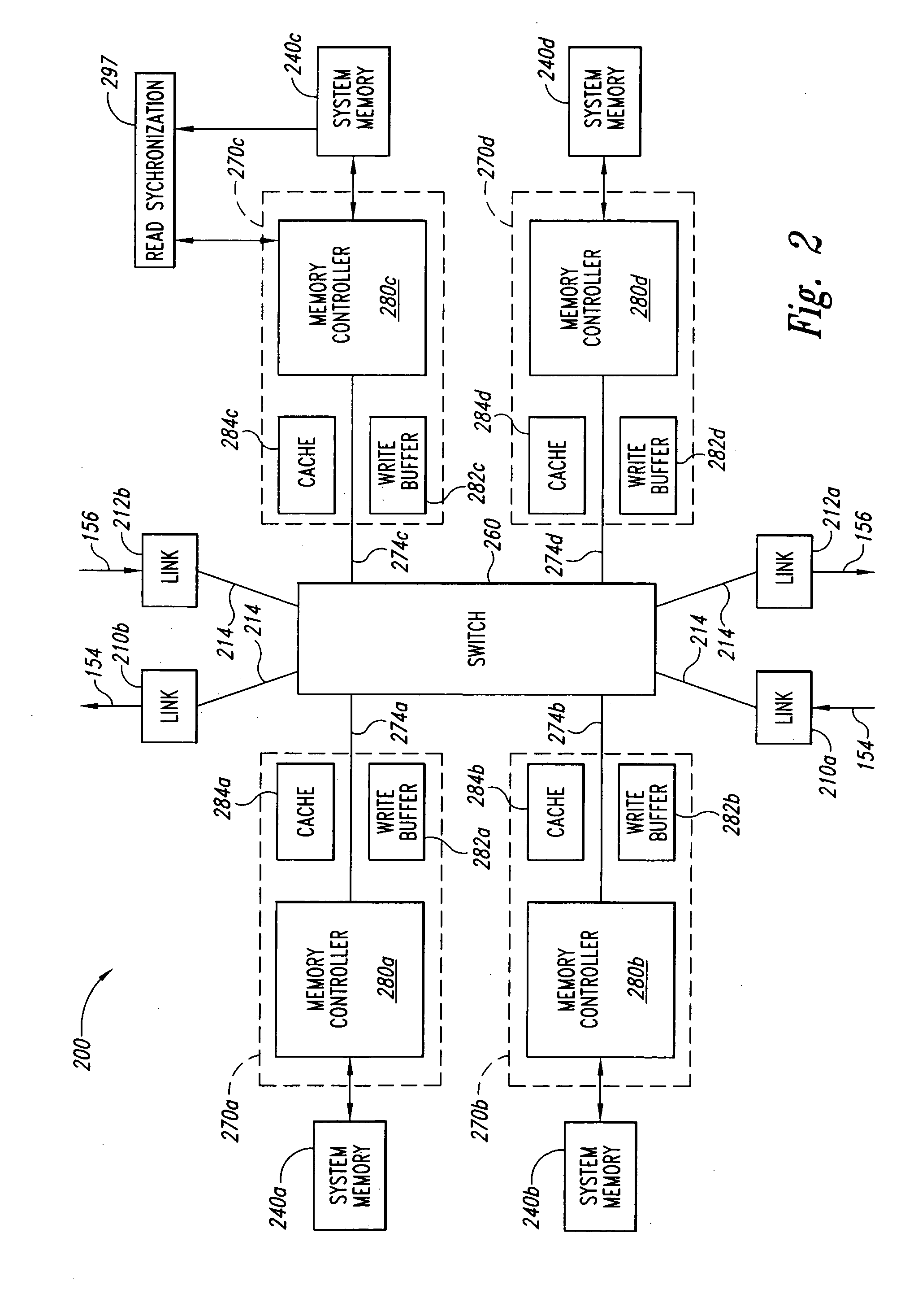
[0022]FIG. 2 illustrates a memory hub 200 in which an embodiment of the present invention is implemented. The memory hub 200 can be substituted for the memory hub 140 of FIG. 1. The memory hub 200 is shown in FIG. 2 as being coupled to system memory 240a-d. The system memory 240a-d is representative of different types of mem...


PUM


Abstract

A system and method for facilitating the adjustment of timing parameters between a memory controller operating in a first clock domain and a memory device operating in a second clock domain. A write pointer and a read pointer are monitored to provide a write-read pointer offset representing the timing between when read data is made available by the memory device and when the read data is retrieved by the memory controller. Based on the write-read pointer offset, adjustment to different timing parameters can be made.

Description

TECHNICAL FIELD [0001] The present invention is related generally to a memory system for a processor-based system, and more particularly, to synchronizing the coupling of read data across different clock domains and providing information related to the timing margin in crossing the different clock domains. BACKGROUND OF THE INVENTION [0002] Computer systems use memory devices, such as dynamic random access memory (“DRAM”) devices, to store data that are accessed by a processor. These memory devices are normally used as system memory in a computer system. In a typical computer system, the processor communicates with the system memory through a processor bus and a memory controller. The memory devices of the system memory, typically arranged in memory modules having multiple memory devices, are coupled through a memory bus to the memory controller. The processor issues a memory request, which includes a memory command, such as a read command, and an address designating the location fr...

Claims


Application Information

Patent Timeline
IPC IPC(8): G06F13/16G11C7/10G11C7/22G11C29/02H04L12/50
CPCG06F13/1684G11C29/50012G11C5/04G11C7/1012G11C7/1039G11C7/1051G11C7/1066G11C7/1069G11C7/1093G11C7/22G11C29/02G11C29/022G11C29/023G11C29/025G11C29/028G06F13/1689
Inventor LABERGE, PAUL A.
Owner MICRON TECH INC
Why Eureka
Try Eureka