Transmitter circuit, receiver circuit, clock data recovery phase locked loop circuit, data transfer method and data transfer system

a technology of clock data and receiver circuit, applied in the field of clock data recovery phase locked loop circuit, transmitter circuit, receiver circuit, data transfer method and data transfer system, can solve the problem of no longer being able to recover accurate digital data, and achieve the effect of reducing errors occurring, eliminating the increase in the cost of the transfer system, and stable data transfer

Active Publication Date: 2005-12-29
THINE ELECTRONICS
View PDF12 Cites 173 Cited by
  • Summary
  • Abstract
  • Description
  • Claims
  • Application Information

AI Technical Summary

Benefits of technology

[0065] According to the present invention, the number of rising edges per one symbol of serial data is fixed to one during blanking periods, making it possible to reduce errors occurring due to waveform degradation when extracting the clock from the serial data, thus realizing stable data transfer.
[0066] With the digital data transfer system of the present invention, serial digital data can be transferred at a high speed from the transmitter unit to the receiver unit by means of a simple configuration using a pair of wires (including the use of an optical fiber). A superior advantage of the present invention is that it does not require a handshake operation using a training signal and an acknowledge signal between the transmitter unit and the receiver unit, which is performed in the prior art. Where an optical fiber is used in the prior art, it is difficult to perform a full-duplex communications operation, which is required in a handshake operation using a training signal and an acknowledge signal. Therefore, the present invention, which does not require a handshake operation, provides a significant advantage where an optical fiber is used as a wire.
[0067] With the digital data transfer system of the present invention, it is possible to transmit low-frequency data (e.g., sound data) during blanking periods (normally, Hsync, Vsync).
[0068] With the digital data transfer system of the present invention, the clock is embedded in serial digital data. As a result, it is not necessary to provide a clock input from a quartz oscillator or an external oscillator to the clock extraction circuit of the receiver unit, which means that even if the size of an image represented by serial digital data changes, the system can automatically follow the changes, and the system is in compliance with plug and play.
[0069] According to the present invention, the receiver unit does not require a reference clock and it is not necessary to transfer data in the reverse direction from the receiver side to the transmitter side, and so it is not necessary to provide a common mode driver on the receiver side and a common mode voltage detection circuit on the transmitter side. It is therefore possible to provide a clock data recovery phase locked loop circuit that eliminates increase in the transfer system cost and decrease in the channel quality.

Problems solved by technology

If the degree of synchronism falls out of a certain range, it is no longer possible to recover accurate digital data.

Method used


Image

  • Transmitter circuit, receiver circuit, clock data recovery phase locked loop circuit, data transfer method and data transfer system
  • Transmitter circuit, receiver circuit, clock data recovery phase locked loop circuit, data transfer method and data transfer system
  • Transmitter circuit, receiver circuit, clock data recovery phase locked loop circuit, data transfer method and data transfer system

Examples


example 1

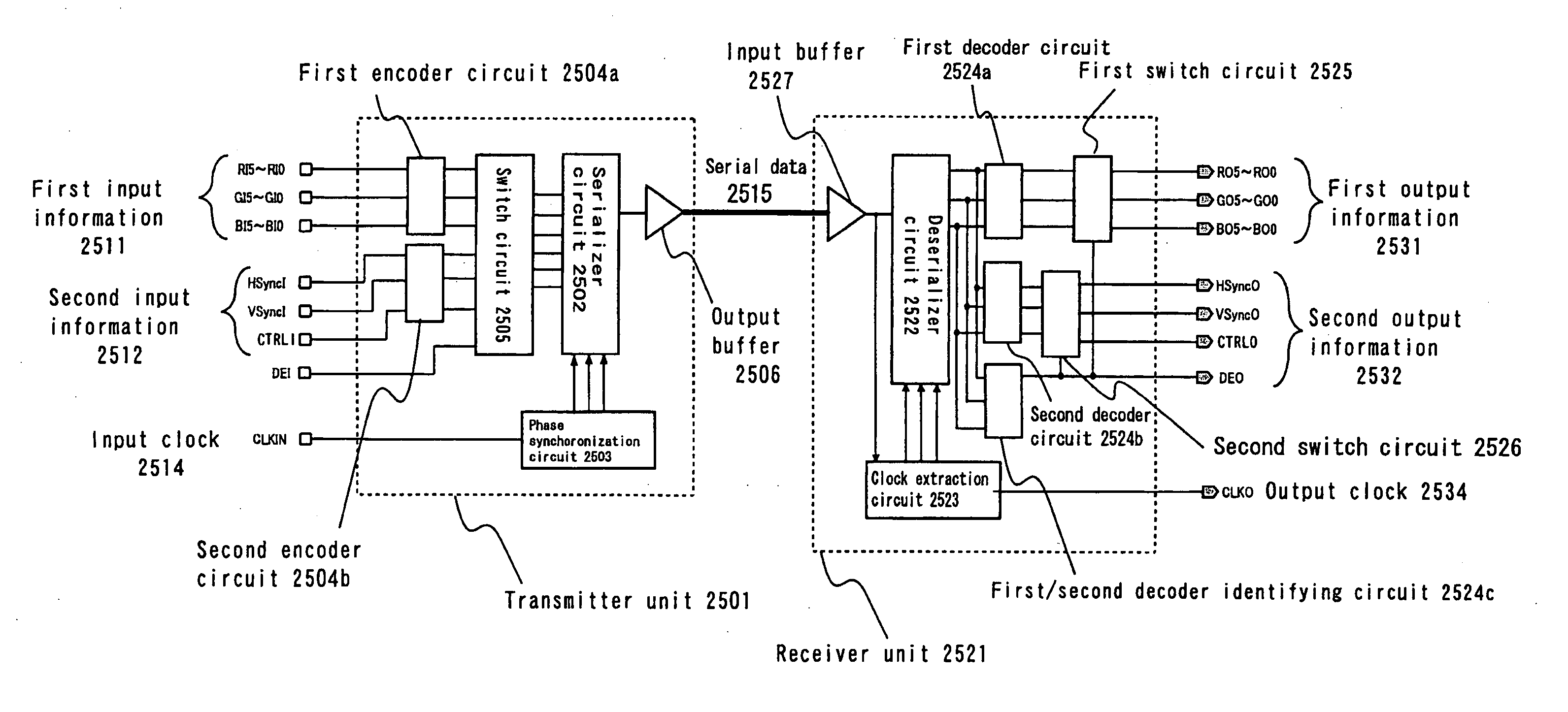
[0276] The present example is directed to an alternative example of the first encoder circuit 2504a in the digital data transfer system of the present invention as described in the embodiment above. Other elements are as described in the embodiment above, and will not be further described below.

[0277] Referring to FIG. 30, FIG. 30 is a diagram illustrating an example of a data error occurring in a serial transfer of digital data. In a data transfer system such as that of the present invention, serial digital data is transferred at a high speed via a pair of wires or cables. Therefore, when data is transferred over a long distance by increasing the wire length or the cable length, or when the wires or cables have poor characteristics, the waveform of the digital data may become smoothed, and bit errors are more likely to occur due to ISI (Intersymbol Interference). Such a data error is significant when low-level data is transferred after high-level data were being transferred for a ...

example 2

[0285] Example 2 is an alternative example of the encoding method of the data transfer system described in the embodiment above. Other elements are as described in the embodiment above, and will not be further described below.

[0286] It is characteristic of the present example that the transmitter unit 2501 includes a DC balance circuit, and the encoding process is performed so as to ensure a DC balance of the serial data. The DC balance circuit counts the total number of “high”s (=1) and the total number of “low”s (=0) in the encoded data, and feeds back to the evaluation function a signal according to the counts. The feedback operation is for selecting encoding mode in the evaluation function so that the total number of “high”s (=1) and the total number of “low”s (=0) in the encoded data converge to the same number. The function of the DC balance circuit as described above will be referred to as a DC balance operation.

[0287] The encoding method in the data transfer system of the ...

example 3

[0300] Example 3 is an alternative example of the clock data recovery phase locked loop circuit (clock extraction circuit) in the data transfer system of the embodiment described above.

[0301] Referring to FIG. 36, FIG. 36 is a hardware block diagram showing a circuit configuration of a clock data recovery phase locked loop circuit (clock extraction circuit) 2600 being a receiver circuit of the present invention. The clock extraction circuit 2600 of the present example is similar to the clock extraction circuit 2523 described in the embodiment above, but further includes a frequency comparison / fine adjustment circuit 80. The same elements as those described in the embodiment above will not be further described below.

[0302] The clock data recovery phase locked loop circuit 2600 of the present example includes the frequency comparison / fine adjustment circuit 80 for performing a finer frequency adjustment (fine frequency adjustment) of the voltage-controlled oscillator 30 after the fr...


PUM


Abstract

[Problems] To realize a reliable and stable transfer of digital data that does not require a reference clock and a handshake operation.
[Means for Solving the Problem] The present invention provides a digital data transfer method for alternately and periodically transferring first information and second information respectively in a first period and in a second period, wherein: an amount of information of the first information per unit time in the first period is greater than an amount of information of the second information per unit time in the second period; and the second information in the first period is transferred as pulse-width-modulated serial data.

Description

TECHNICAL FIELD [0001] The present invention relates to a transmitter circuit and a receiver circuit for transferring parallel digital data while serializing the digital data, an encoder circuit for use in a transmitter circuit, and a data transfer method and a data transfer system using the same. [0002] The present invention also relates to a receiver circuit used in a serial data transfer system in which parallel digital data is transferred while being serialized, and more particularly to a clock data recovery phase locked loop circuit (also referred to as a CDRPLL circuit or a clock extraction circuit) in a receiver unit used in a serial data transfer system. BACKGROUND ART [0003] In recent years, for the transfer of digital data between devices, there has been an increasing demand for serial transfer at higher speeds. Serial transfer of digital data has advantages over parallel transfer of digital data, such as the ability to reduce wires between devices as much as possible, thu...

Claims


Application Information

Patent Timeline
Patent Type & Authority Applications(United States)
IPC IPC(8): H03D3/18H03K9/08H03L7/087H03L7/091H03L7/113H03M9/00H04B14/04H04L7/033H04L25/45H04L25/49H04N11/04
CPCH03K7/10H03L7/087H03L7/091H04L25/4902H04L7/033H04L25/45H03L7/113H04L25/49H03M9/00
Inventor OZAWA, SEIICHIOKAMURA, JUN-ICHIISHIZONE, YOHEIMIURA, SATOSHI
Owner THINE ELECTRONICS
Why Eureka
Try Eureka