Protective layer of gas discharge display device and method of forming the same

a technology of display device and protective layer, which is applied in the manufacture of electric discharge tubes/lamps, electrode systems, inorganic insulators, etc., can solve the problems of impracticality of display devices, and achieve the effects of reducing the increase of discharge voltage, shortening the discharge lag time, and high brightness

Inactive Publication Date: 2005-12-29
SAMSUNG SDI CO LTD
View PDF4 Cites 12 Cited by
  • Summary
  • Abstract
  • Description
  • Claims
  • Application Information

AI Technical Summary

Benefits of technology

[0010] The present invention provides a protective layer which reduces an increase in discharge voltage due to the use of an increased amount of a Xe gas for high brightness, and at the same time, provides a shorter discharge lag time for single scan. The present invention also provides a composition for forming the protective layer, a method of forming the protective layer, and a plasma display panel (PDP) including the protective layer.

Problems solved by technology

However, this technique is impractical in display devices due to very high discharge initiation voltage.

Method used


Image

  • Protective layer of gas discharge display device and method of forming the same
  • Protective layer of gas discharge display device and method of forming the same
  • Protective layer of gas discharge display device and method of forming the same

Examples


example 1

[0074] 100 mole % of MgO, 2 mole % of Li2CO3, and 2 mole % of GeO2 were placed in a mixer and uniformly mixed for 5 hours or more. The resultant mixture was placed in a crucible and heated in an electric furnace at 500° C. for 10 hours. The resultant product was compression-molded into pellets and sintered at 1,300° C. to prepare a deposition source.

[0075] Meanwhile, address electrodes made of copper were formed on a rear substrate with a thickness of 2 mm by photolithography. The address electrodes were covered with PbO glass to form a rear dielectric layer with a thickness of 20 μm. Then, the rear dielectric layer was coated with a BaAl12O19:Mn green-emitting phosphor.

[0076] Bus electrodes made of copper were formed on a front substrate with a thickness of 2 mm by photolithography. The bus electrodes were covered with PbO glass to form a front dielectric layer with a thickness of 20 μm. Then, the deposition source was deposited on the front substrate by e-beam evaporation to for...


PUM

PropertyMeasurementUnit
bandgap energyaaaaaaaaaa
sizeaaaaaaaaaa
thicknessaaaaaaaaaa

Abstract

Provided is a protective layer formed using at least one selected from the group consisting of a magnesium oxide and a magnesium salt and at least one selected from the group consisting of a lithium salt, a lithium oxide, a germanium oxide, and a germanium element. Provided is also a composition for forming a protective layer. When the composition is used for a protective layer of a gas discharge display device, an electrode or a dielectric can be protected from plasma ions generated by discharge of a mixed gas of Ne+Xe or He+Ne+Xe, a lower discharge voltage and a shorter discharge lag time can be obtained.

Description

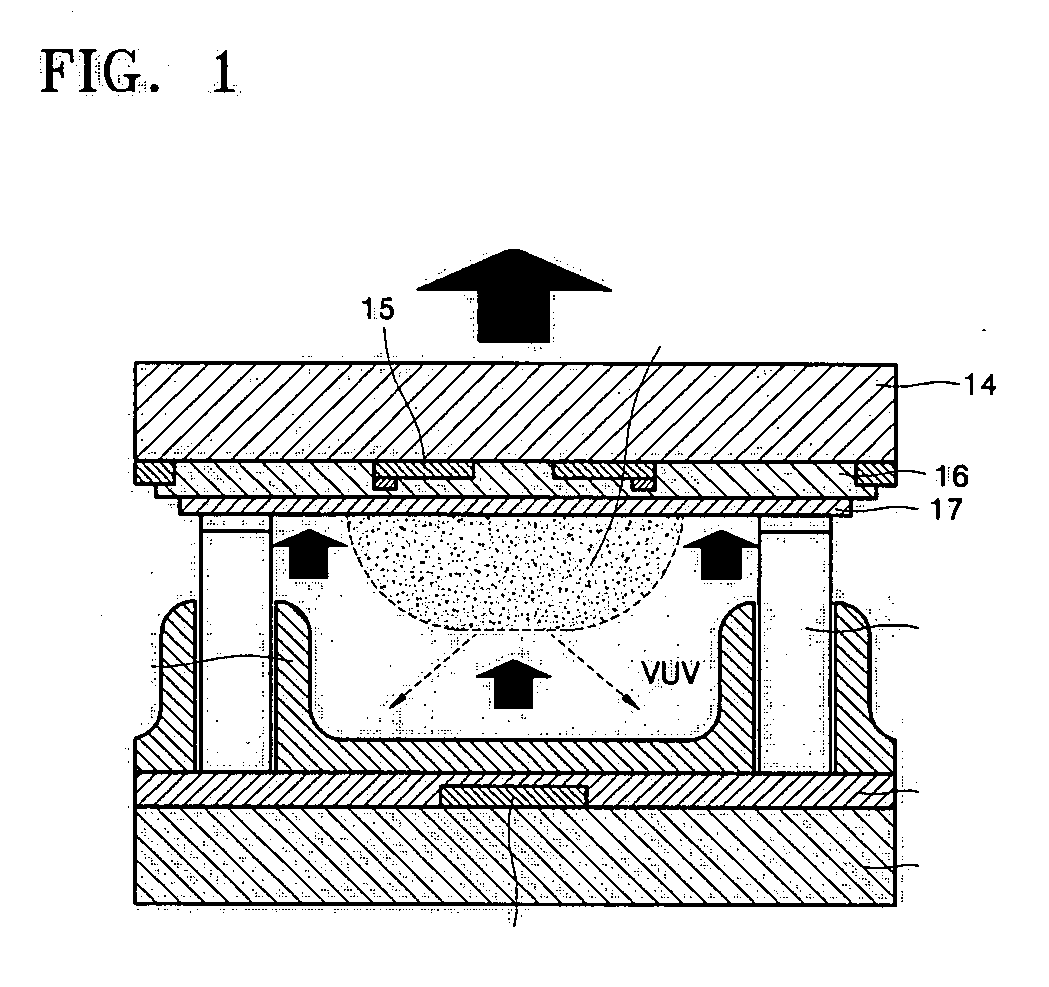
CROSS-REFERENCE TO RELATED APPLICATIONS [0001] This application claims the priority of Korean Patent Application No. 10-2004-0048655, filed on Jun. 26, 2004, in the Korean Intellectual Property Office, the disclosure of which is incorporated herein in its entirety by reference. FIELD OF THE INVENTION [0002] The present invention relates to a protective layer of a gas discharge display, and more particularly, to a dielectric protective layer which has excellent discharge characteristics and a method of forming the same. DESCRIPTION OF THE RELATED ART [0003] Plasma display panels (PDPs) are self-emission devices that can be easily manufactured as large displays, and have good display quality and rapid response speed. In particular, because of their thinness, PDPs have received much interest as wall-hanging displays, like liquid crystal displays (LCDs). [0004]FIG. 1 illustrates a PDP pixel. Referring to FIG. 1, discharge sustain electrodes (15 for each), each including a pair of a firs...

Claims


Application Information

Patent Timeline
Patent Type & Authority Applications(United States)
IPC IPC(8): B05D5/12C04B35/043H01J17/49H01B3/10H01J9/02H01J11/22H01J11/24H01J11/34H01J11/40
CPCC04B35/043C04B2235/3203H01J11/40C04B2235/72H01J11/12C04B2235/3287H01J9/02
Inventor LEE, MIN-SUKCHOI, JONG-SEOOH, MIN-HOKIM, JAE-HYUKSUH, SOON-SUNG
Owner SAMSUNG SDI CO LTD
Why Eureka
Try Eureka