Composition for forming organic insulating film and method for forming pattern of organic insulating film using the same

a technology of organic insulating film and organic insulating film, which is applied in the direction of thermoelectric device junction material, electrical apparatus, and semiconductor devices. it can solve the problems of inability to replace inorganic insulating film, inability to meet the requirements of plastic substrate application, etc., to achieve high charge carrier mobility and simplify the overall procedure

Inactive Publication Date: 2006-01-12
SAMSUNG ELECTRONICS CO LTD
View PDF5 Cites 38 Cited by
  • Summary
  • Abstract
  • Description
  • Claims
  • Application Information

AI Technical Summary

Benefits of technology

[0015] Therefore, embodiments of the present invention has been made in view of the above problems of the prior art, and it is an object of the embodiments of the present invention to provide a method for forming a pattern of an organic insulating film with resistance to organic solvents used in subsequent processes in a simple manner without involving any photoresist process, thereby simplifying the overall procedure and eventually enabling fabrication of an organic thin film transistor with high charge carrier mobility by all wet processes.

Problems solved by technology

However, these inorganic oxide materials do not have a significant advantage over conventional silicon materials in terms of processing.
However, since these organic insulating films exhibit unsatisfactory device characteristics over inorganic insulating films, they are unsuitable to replace inorganic insulating films.
However, this attempt is limited in its application to plastic substrates since a temperature as high as 200° C. is required to crosslink the PVP (Journal of Applied Physics 2003, 93, 2977 & Journal of Applied Physics 2002, 81, 289).
Accordingly, the compositions are very limited in their use.
The choice of unsuitable compositions inevitably causes poor electrical properties and makes the fabrication of organic thin film transistors by all wet processes difficult.
However, this method has the limitation that it is not applicable to organic thin film transistors.
However, the application of this method is limited to patterns of source / drain electrodes.

Method used


Image

  • Composition for forming organic insulating film and method for forming pattern of organic insulating film using the same
  • Composition for forming organic insulating film and method for forming pattern of organic insulating film using the same
  • Composition for forming organic insulating film and method for forming pattern of organic insulating film using the same

Examples


example 1

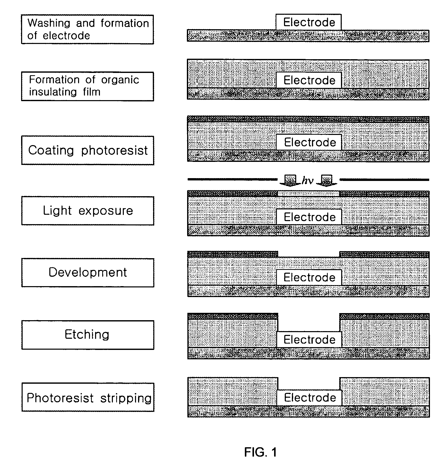
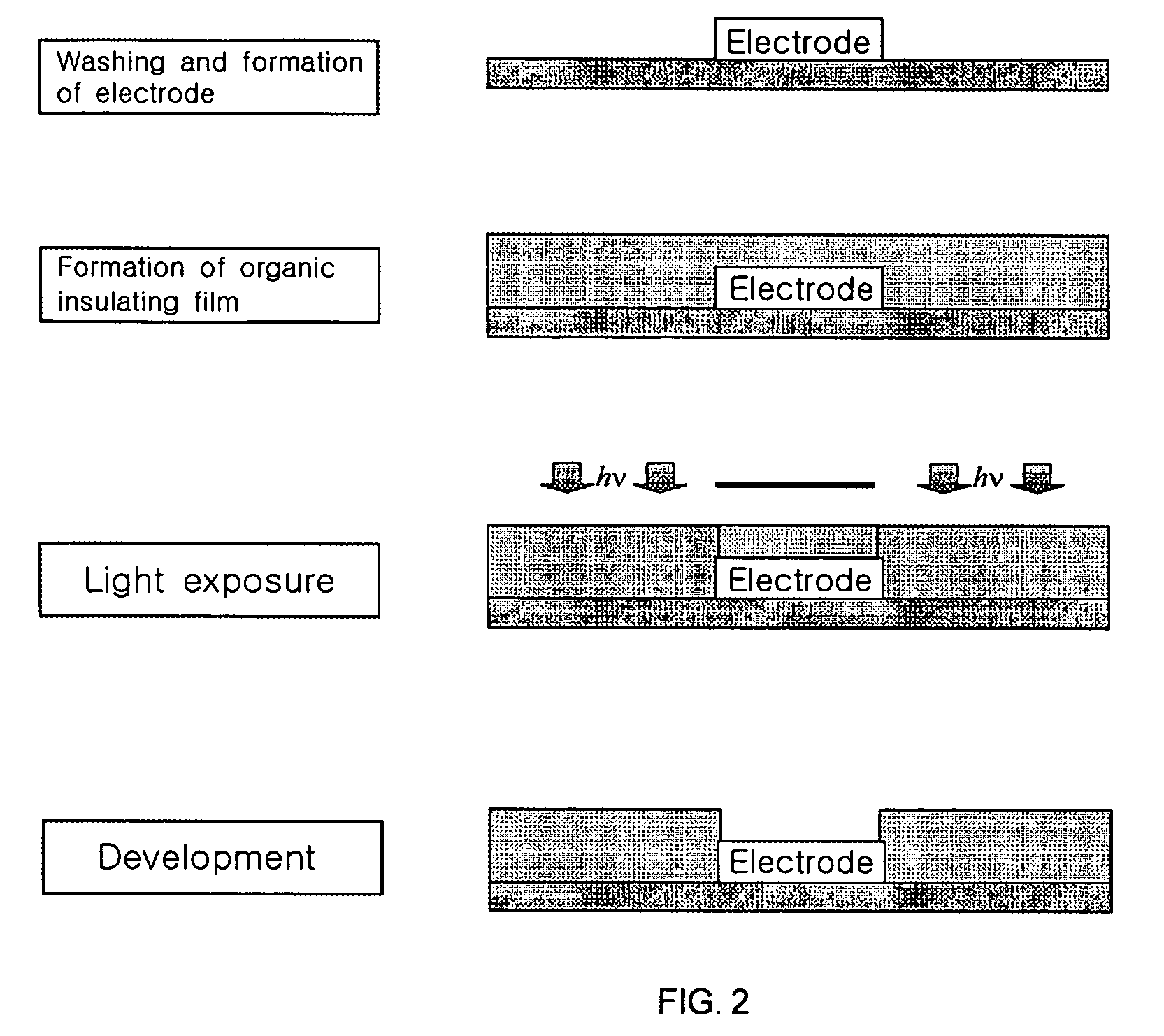
[0071] (1) Formation of Pattern of Organic Insulating Film

[0072] The composition for forming an organic insulating film prepared in Preparative Example 1 was spin-coated at 2,000 rpm on a glass substrate to form an 8,000 Å thick organic insulating film, and soft-baked at 100° C. for 5 minutes. Thereafter, the organic insulating film was irradiated with UV light (100 mJ / cm2) in a UV exposure system through a photomask having a desired shape, and hard-baked at 100° C. for 10 minutes. Next, the exposed inorganic insulating film was developed using 1-methyl-2-pyrrolidone as an organic developing solution to remove the unexposed region, thereby forming the pattern of the organic insulating film shown in FIG. 4.

[0073] (2) Fabrication of Organic Thin Film Transistor

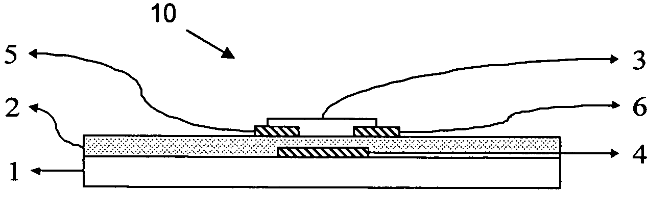
[0074] An 800 Åthick gate electrode was formed using molybdenum (Mo) on a glass substrate, and then a pattern of an organic insulating film on an electrode for connection to a driving circuit was formed in the same manner as ...

example 2

[0076] (1) Formation of Pattern of Organic Insulating Film

[0077] A pattern of an organic insulating film was formed in the same manner as in Example 1, except that the composition prepared in Preparative Example 2 was used.

[0078] (2) Fabrication of Organic Thin Film Transistor

[0079] An organic thin film transistor was fabricated in the same manner as in Example 1, except that the pattern formed in Example 2 (1) was used.


PUM


Abstract

A photo-patternable composition for forming an organic insulating film which includes (i) a functional group-containing monomer, (ii) an initiator generating an acid or a radical upon light irradiation, and (iii) an organic or inorganic polymer. Further disclosed is a method for forming a pattern of an organic insulating film using the composition. Since an organic insulating film can be simply patterned without involving any photoresist process, the overall procedure is simplified and eventually an organic thin film transistor with high charge carrier mobility can be fabricated by all wet processes.

Description

BACKGROUND OF THE INVENTION [0001] This non-provisional application claims priority under 35 U.S.C. §119(a) on Korean Patent Application No. 2004-46177 filed on Jun. 21, 2004, which is herein expressly incorporated by reference, and on Korean Patent Application No. 2005-47107 filed on Jun. 2, 2005, which is herein expressly incorporated by reference. [0002] 1. Field of the Invention [0003] The embodiments of the present invention relate to a composition for forming an organic insulating film and a method for forming a pattern of an organic insulating film using the composition. More particularly, the embodiments of the present invention relate to a photo-patternable composition for forming an organic insulating film which comprises: (i) a functional group-containing monomer; (ii) an initiator generating an acid or a radical upon light irradiation; and (iii) an organic or inorganic polymer, and a method for forming a pattern of an organic insulating film using the composition. [0004]...

Claims


Application Information

Patent Timeline
Patent Type & Authority Applications(United States)
IPC IPC(8): H01L29/08
CPCH01L21/0274H01L51/052H01L21/31133H10K10/471
Inventor SHIN, JUNG HANLEE, TAE WOOKOO, BON WONLEE, BANG LINLEE, SANG YOON
Owner SAMSUNG ELECTRONICS CO LTD
Why Eureka
Try Eureka