Waveguide plate and process for its production and microtitre plate

a waveguide plate and microtitre technology, applied in the field of waveguide plates, can solve the problems of inability to avoid stitching errors during inscribing by means of electron beams, requiring very long processing times, and requiring a large amount of processing time, etc., to achieve high precision, high optical element precision, and successive exposure of different parts

Inactive Publication Date: 2006-01-12
OERLIKON TRADING AG TRUEBBACH
View PDF16 Cites 21 Cited by
  • Summary
  • Abstract
  • Description
  • Claims
  • Application Information

AI Technical Summary

Benefits of technology

[0013] Furthermore, it is the object of the invention to provide a process for producing a waveguide plate according to.the invention, which permits the creation of large gratings in particular having long parallel lines with great precision, provides freedom of design with regard to the arrangement of the gratings and is simple and economical. The process according to the invention furthermore permits the production of large series of waveguide plates of constant quality and having optical properties, such as coupling efficiencies and in particular coupling angles, which are within narrow limits. The process according to the invention also permits the production of large series of optical elements of constant quality and with optical properties such as coupling efficiencies and, in particular, coupling angles which are constant within narrow limits.
[0016] Additionally, a highly precise optical element is to be provided such as can be produced by the process according to the invention. In particular, the optical element can be formed as a waveguide plate or an evanescent field sensor plate or as a microtitre plate based on such a plate. In view of the narrow limits within which, even in long gratings, the coupling angle varies, it is possible to simultaneously illuminate and read out larger parts of the waveguide plate or evanescent field sensor plate or microtitre plate. Successive exposure of different parts of the waveguide plate or the evanescent field sensor plate or microtitre plate is also simplified since reoptimization of the relative angular position of this plate and the exposing unit is not required or in any case greatly simplified.
[0017] The optical element can also be formed as an optical coupler for communications technology. In this case, the high precision present even in large grating structures guarantees excellent filter characteristics, and particularly a very-narrow-band selection of individual wavelengths, so that, for instance, a wavelength multiplexing involving very closely spaced wavelengths is possible, which raises the transmission capacity.

Problems solved by technology

Greater lengths are possible but require very long processing times. In practice, gratings of more than 1 mm2 can hardly be produced with reasonable effort and good accuracy.
In particular, stitching errors during inscribing by means of electron beams cannot be avoided.
All plates described above are produced by processes with which no satisfactory uniformity of the coupling grating can be achieved, so that the coupling angle varies relatively widely.
The filter characteristics are unsatisfactory and not sufficient, for instance, for selectively filtering a particular wavelength from a group of very closely spaced wavelengths, when the plate is used as an optical coupler in communications technology.
Some of the processes described are also very laborious or do not allow very large numbers of pieces of constant quality to be made.

Method used


Image

  • Waveguide plate and process for its production and microtitre plate
  • Waveguide plate and process for its production and microtitre plate
  • Waveguide plate and process for its production and microtitre plate

Examples


example 1

Design of A Waveguide Plate According To the Invention And Arrangement of Sample Compartments To Be Formed By the Combination With Said Waveguide Plate

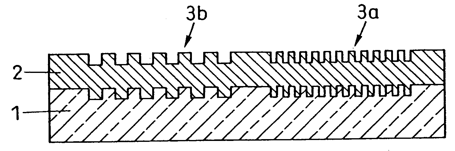
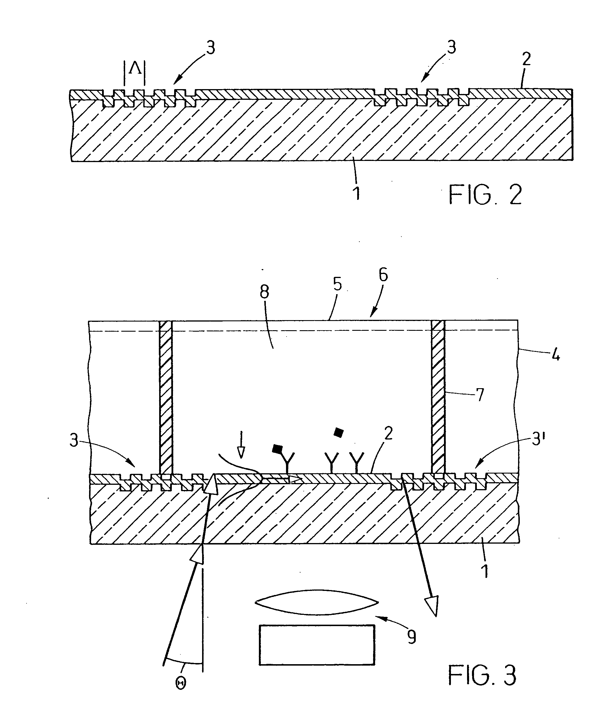
[0128] The waveguide plate according to the invention (FIGS. 1, 2 are schematically and not according to scale) comprises a glass substrate, for example of glass AF 45 from Schott DESAG, with dimensions of 102 mm×72 mm and a thickness of 0.7 mm, carrying on one surface a waveguiding layer 2 of Ta2O5 of 150 nm thickness. The refractive index is, dependent on the manufacturing method, for example 2.11 at 633 mn. Besides Ta2O5, also other materials are suited for the waveguiding layer, especially Nb2O5, TiO2, ZrO2, Al2O3, SiO2-TiO2, HfO2, Y2O3, SiOxNy, Si3N4, HfOxNy, AIOx,Ny, TiOxNy, MgF2 or CaF2.

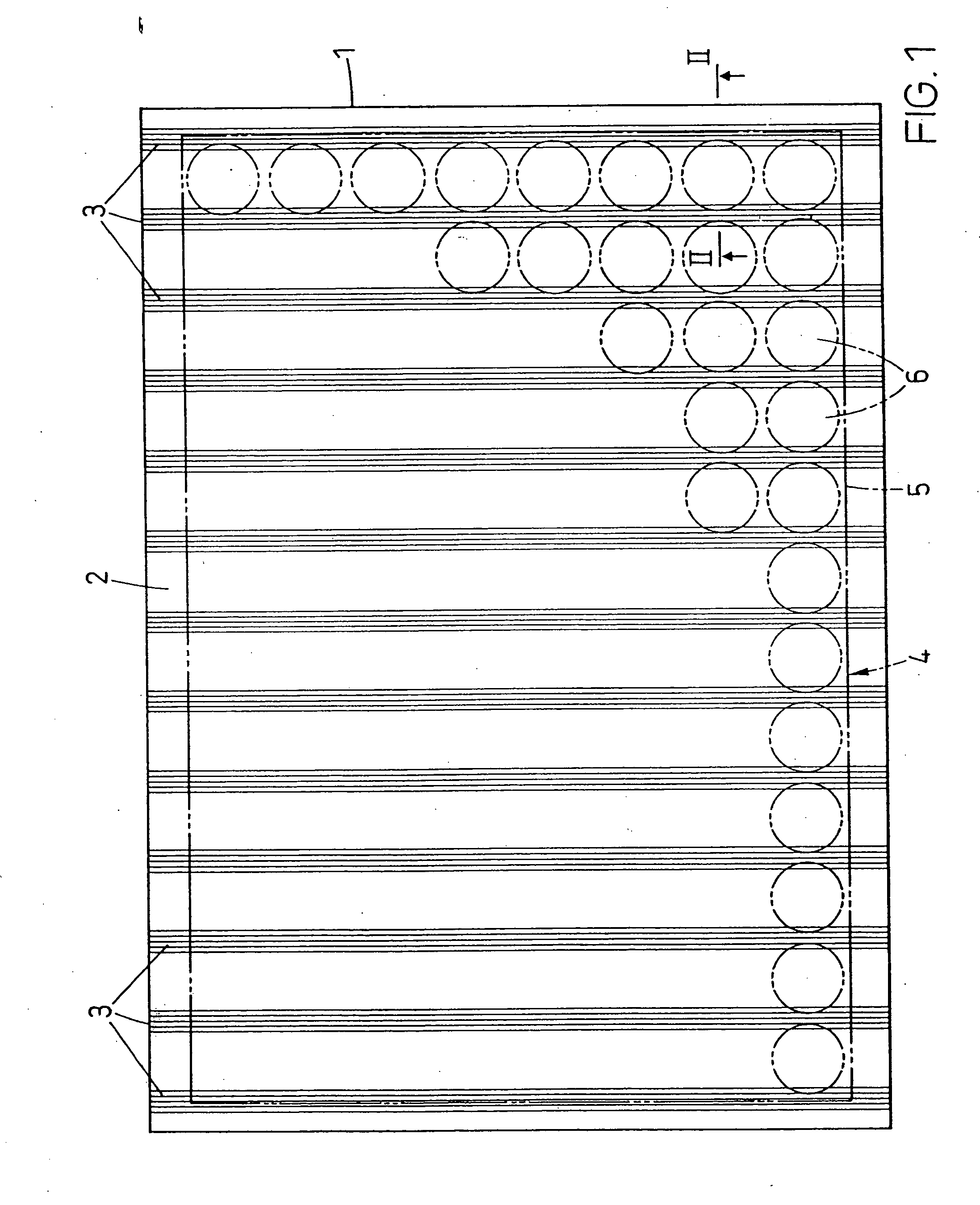
[0129] On the surface carrying the waveguiding layer 2, several coupling grating strips 3 are arranged in parallel to and separate from each other, extending in parallel lines over the whole width of the waveguide plate. The width of each of t...

example 2

Characterization of A Waveguide Plate According To the Invention

[0132] A waveguide plate according to Example I (waveguiding layer of Ta2O5, refractive index n=2.11 at 633 nm) is characterized. The waveguide plate is designed for use as a base plate for an arrangement of 96 sample compartments (provided as flowthrough cells) in a geometrical arrangement according to FIG. 1 (8 rows×12 columns of sample compartments). For the characterization of the physical properties of the waveguide plate, the following parameters shall be determined: (a) coupling angle and (b) the halfwidth of the resonance angle for maximum incoupling, (c) the lateral position (“x-position”) for optimum incoupling on a coupling grating strip and (d) its halfwidth, (e) the incoupling efficiency, (f) the number and size of scattering centers per area unit of the region of the sample compartments, analysis of (g) the excitation light profile for the region of the sample compartments, (h) background luminescence at ...


PUM

PropertyMeasurementUnit
thicknessaaaaaaaaaa
thicknessaaaaaaaaaa
grating depthaaaaaaaaaa

Abstract

A waveguide plate and a process for making the waveguide plate with a plate-like glass substrate (1), carrying a waveguiding layer (2), with at least one coupling grating on the surface carrying said waveguiding layer (2), which coupling grating is formed as a grating of lines with a period between 150 nm and 1000 nm, the extension of said grating being at least 5 cm with lines parallel to one another, wherein the coupling angle (θ) varies by not more than 0.1° / cm along a line of said grating and wherein the absolute value of the deviation of the coupling angle (θ) on said waveguide plate, from a predefined desired value, does not exceed 0.5°. The deviation from the average value of the coupling angle does not exceed 0.3°, preferably not 0.15° on the whole waveguide plate. The waveguide plate is suitable as part of a sensor platform and of an arrangement of sample compartments for chemo-and bioanalytical investigations in order to produce a coupling grating formed as a line grating with a grating period between 100 nm and 2500 nm.

Description

CROSS-REFERENCE TO RELATED APPLICATIONS [0001] This application is a continuation-in-part of U.S. application Ser. No. 09 / 497,129 filed on Feb. 3, 2000.BACKGROUND OF THE INVENTION [0002] The invention relates to a waveguide plate and a process for its production and a microtitre plate comprising such a waveguide plate and as used, for example, for analytical purposes in the biochemical and medical sector, as well as a sensor platform based on a waveguide plate, an evanescent field sensor plate, according to the invention as well as arrangements of sample compartments, with a waveguide plate or a sensor platform according to the invention as a boundary surface of said arrangement of sample compartments. The invention also relates to an optical coupler and a device for monitoring such a coupler. [0003] The process according to the invention is suitable for producing optical elements with grating structures. Evanescent field sensor plates and microtitre plates produced according to the...

Claims


Application Information

Patent Timeline
Patent Type & Authority Applications(United States)
IPC IPC(8): G02B6/34G01N21/55G01N21/77G02B6/12G02B6/124
CPCG01N21/552G01N21/7743G02B6/124G02B2006/12147G02B6/34G02B2006/12107G02B6/136G01N21/648
Inventor MAISENHOELDER, BERNDEDLINGER, JOHANNESHEINE-KEMPKENS, CLAUSPAWLAK, MICHAELDUVENECK, GERT
Owner OERLIKON TRADING AG TRUEBBACH
Why Eureka
Try Eureka