Method of forming wiring pattern

a technology of wiring pattern and wire pattern, which is applied in the direction of non-linear optics, double resist layers, instruments, etc., can solve the problems of poor ink positioning accuracy, increased manufacturing cost, and increased manufacturing cost, so as to reduce the influence of ink positioning accuracy, prevent the generation of voids in films, and use ink materials more efficiently

Active Publication Date: 2006-01-12
HANNSTAR DISPLAY CORPORATION
View PDF2 Cites 14 Cited by
  • Summary
  • Abstract
  • Description
  • Claims
  • Application Information

AI Technical Summary

Benefits of technology

[0027] Thus, it is possible to reduce the influence on the accuracy in positioning of the inks, to form a fine wiring pattern using an inkjet system, and to use an ink material more efficiently.
[0028] Furthermore, the method of the present invention for forming a wiring pattern allows the photoresist to have a reverse tapered cross-section, and therefore the wiring pattern can be formed to have forward tapered cross-sections.
[0029] In this way it is possible to prevent generation of voids in films provided between layers that are arranged above the layer where the wiring pattern in question are formed. Also, it is possible to prevent breakage of a wiring pattern that are provided in upper layers of the wiring.

Problems solved by technology

When TFTs are intended to be formed on the substrate in this way, the manufacturing cost is increased due to the use of vacuum systems in the sputtering process.
In the above-described method of forming a wiring pattern disclosed in patent document 1, an ink material is applied on the entire surface of the substrate, and therefore the manufacturing cost is increased.
However, this inkjet system has poor accuracy in positioning of inks, and is not generally suited for the formation of fine patterns.
For this reason, consumption of materials may be increased when the ink is applied by spin coating, and the ink may be applied on the unnecessary portions of a substrate.
Thus, materials are not efficiently used and the manufacturing cost is increased.
However, conventional inkjet systems have poor accuracy in positioning of inks, and are not suited for the formation of fine wiring patterns.
Accordingly, there is a problem that the shape and thickness of the water repellent film that needs to be removed cannot be controlled accurately.
As a result, the shape of a wiring pattern, reflecting the portions of the water repellent film that have been removed, cannot be controlled accurately.
In addition, when multilayered wiring patterns are to be formed, a wiring pattern in the lower layers are damaged by the laser beam, and voids are generated in insulating films provided between the upper and lower layers of a wiring pattern.

Method used


Image

  • Method of forming wiring pattern
  • Method of forming wiring pattern
  • Method of forming wiring pattern

Examples


embodiment 1

Exemplary Typical Embodiment 1

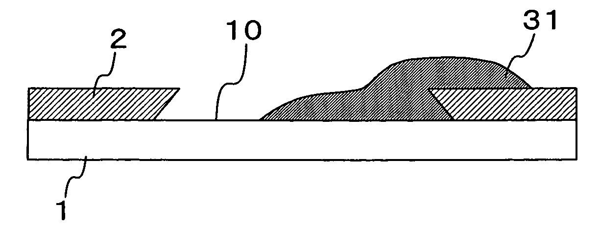
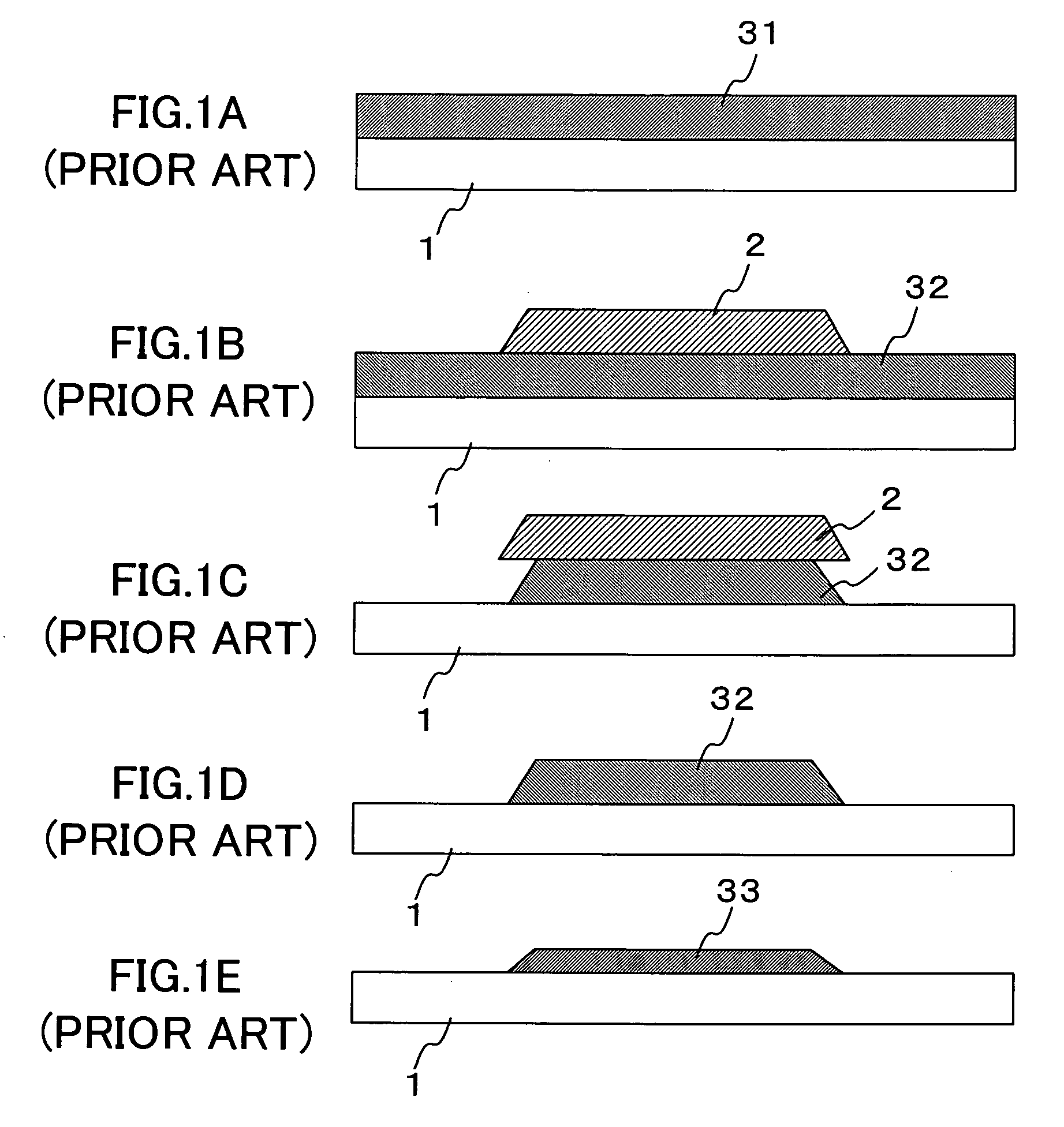
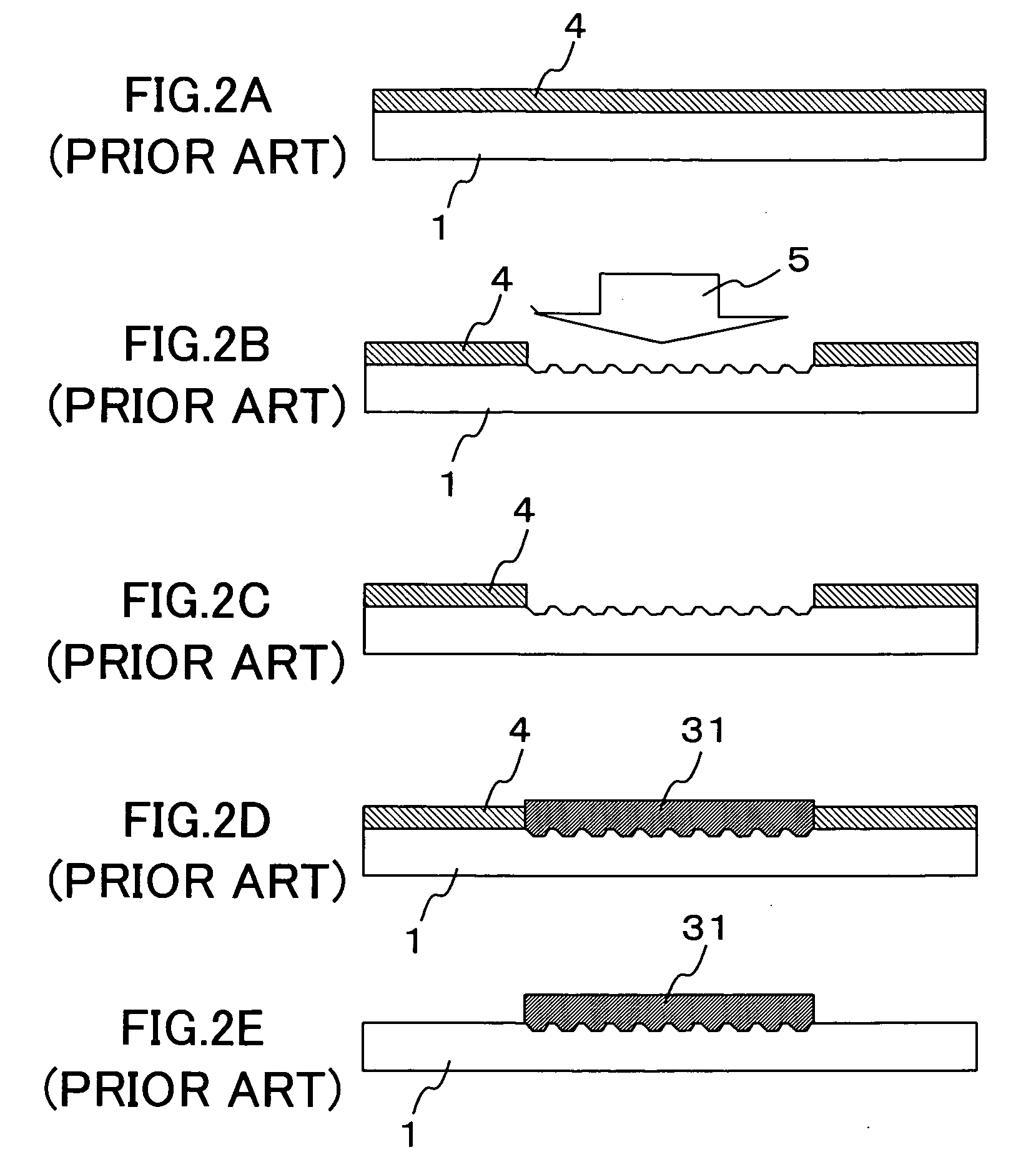
[0039] Hereinafter, a first embodiment of the present invention will be described with reference to the drawings, in which the formation of a gate wiring on a panel substrate of a liquid crystal display device is taken as an example. First, as shown in FIGS. 3A and 4A, a photoresist 2 having a pattern as shown is formed on an insulating substrate 1 such as a glass substrate to partition it into an wiring region 10 for a gate wiring. This process is the first step of forming a wiring pattern, and is a lithography process through which the wiring region 10 is formed on the insulating substrate 1, the entire surface of which has been coated with the photoresist 2, by irradiating it with light or laser beams.

[0040] The photolithography process includes an application step of applying the photoresist 2 onto the entire surface of the substrate 1, an exposure step of exposing the photoresist 2, corresponding to regions other than the wiring region 10, to ligh...

embodiment 2

Exemplary Typical Embodiment 2

[0053] Next, a second embodiment of the method of the present invention for forming a wiring pattern will be described with reference to FIG. 5, in which the formation of a gate wiring on a panel substrate of a liquid crystal display device is taken as an example. In this embodiment, as shown in FIG. 5, only the cross-sectional views of a substrate 1 and a photoresist are shown, which are equivalent to those shown in FIG. 4A, described in the first embodiment. Because the cross-sectional views of the substrate 1, a photoresist formed thereon, and an wiring formed of an ink are similar to those described in FIGS. 4B to 4F, they are not illustrated in FIG. 5.

[0054] In the first embodiment, a negative photoresist with a reverse tapered cross section is used as the photoresist applied on the insulating substrate 1 in the photolithography process as the first step. In this embodiment, instead of using this negative photoresist, a positive photoresist is use...


PUM


Abstract

A photoresist pattern is formed on an insulating substrate so that it has a reverse tapered cross section and a reverse pattern of a wiring pattern to be formed. Next, a nanoparticles-containing ink is injected on a wiring region using an inkjet system, followed by a leveling process, a drying process, a resist separation process and a baking process. Thus a wiring pattern is formed.

Description

BACKGROUND OF THE INVENTION [0001] 1. Field of the Invention [0002] The present invention relates to a method of forming a wiring pattern on panel substrates of display devices such as liquid crystal display devices and plasma displays. Specifically, the present invention relates to a method of forming a wiring pattern using inks containing metallic nanoparticles. [0003] 2. Description of the Related Art [0004] Conventionally, various processes, that is, a sputtering process, a photolithography process and an etching process are used to form a wiring pattern on substrates that are used for liquid crystal display devices and the like and include thin film transistors (TFTs) arranged in an array. [0005] For example, the sputtering process is the process for adhering a metal film or the like, constituting a wiring pattern, to the substrate, and the photolithography process is the process for forming a predetermined pattern for a wiring pattern. In addition, the etching process is the p...

Claims


Application Information

Patent Timeline
Patent Type & Authority Applications(United States)
IPC IPC(8): H01L21/44
CPCH01L21/288H01L21/76838H05K3/125H05K2203/0594H05K2203/013H05K2203/0568H05K2203/0577H05K3/1258B82Y30/00G02F1/136
Inventor TANAKA, HIROAKI
Owner HANNSTAR DISPLAY CORPORATION
Why Eureka
Try Eureka