Semiconductor device and method for fabricating the same

Inactive Publication Date: 2006-01-19
PANASONIC CORP
View PDF7 Cites 11 Cited by
  • Summary
  • Abstract
  • Description
  • Claims
  • Application Information

AI Technical Summary

Benefits of technology

[0011] It is an object of the present invention to reduce film formation variations and polishing amount variations of an interlayer dielectric de

Problems solved by technology

However, the above-mentioned known semiconductor devic

Method used


Image

  • Semiconductor device and method for fabricating the same
  • Semiconductor device and method for fabricating the same
  • Semiconductor device and method for fabricating the same

Examples


embodiment 1

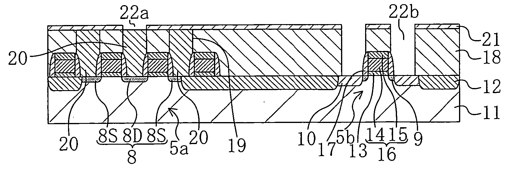
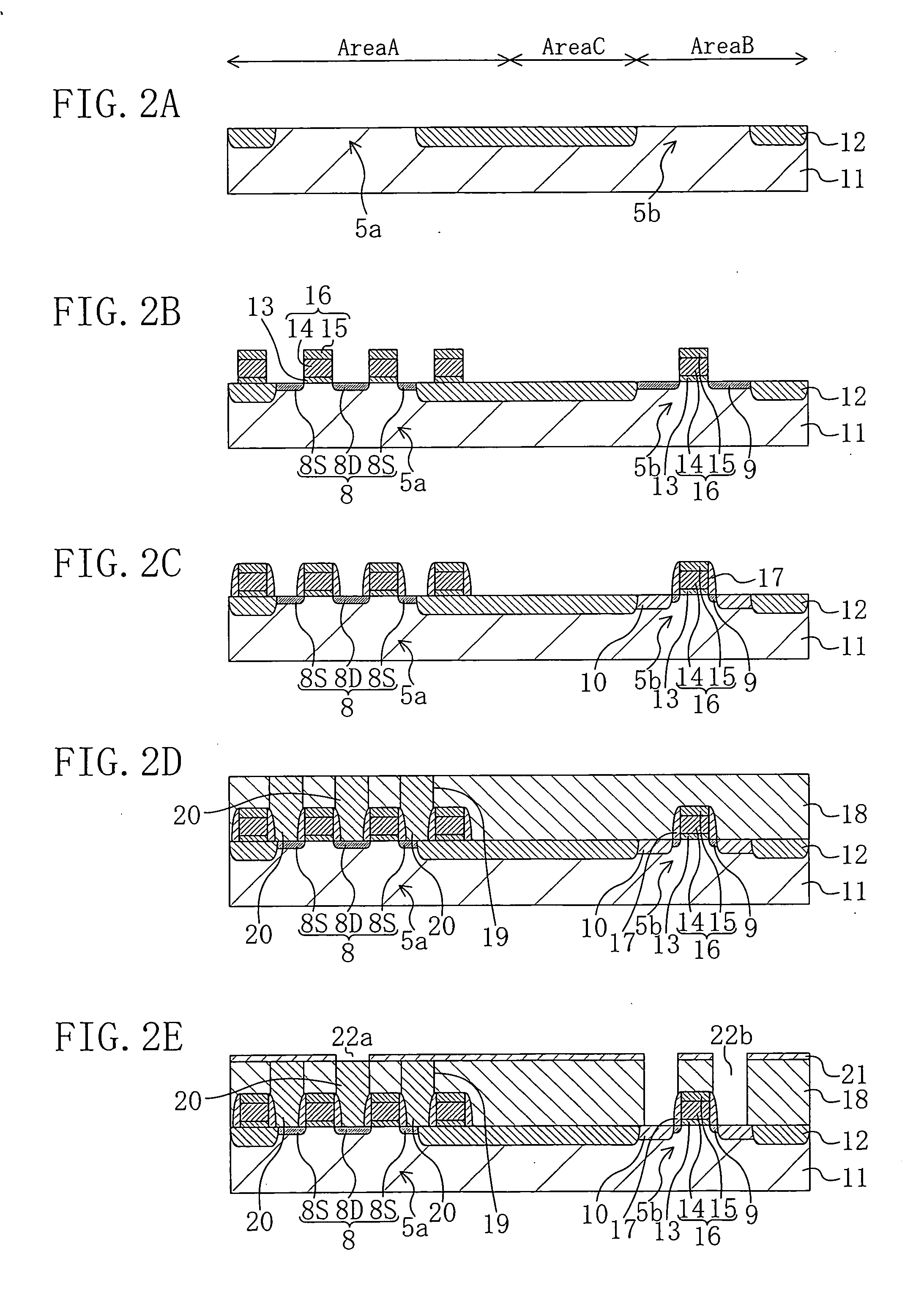
[0040] A method for fabricating a semiconductor device according to a first embodiment of the present invention will be described hereinafter with reference to the drawings. FIGS. 2A through 4C and 5 are cross-sectional views showing process steps in the method for fabricating a semiconductor device according to the first embodiment of the present invention.

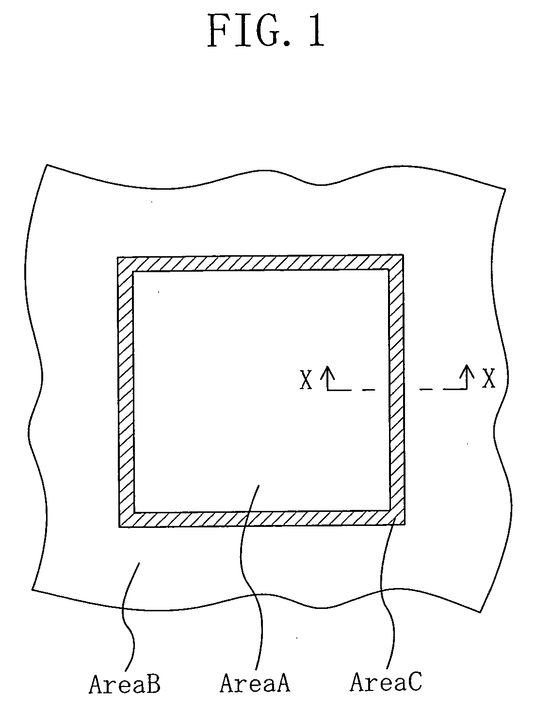
[0041] According to a method for fabricating a semiconductor device of the present invention, first, in a process step shown in FIG. 2A, a shallow trench isolation region 12 is formed in a semiconductor substrate 11 to surround respective active regions 5a and 5b of a memory cell area AreaA and a peripheral circuit area AreaB. Subsequently, desired ion implantation is carried out, thereby forming well diffusion layers and threshold-voltage-controlling impurity layers (both not shown) in the memory cell area AreaA and the peripheral circuit area AreaB. In this case, a p-type well is formed in the memory cell area AreaA, and a p-t...

embodiment 2

[0057] A method for fabricating a semiconductor device according to a second embodiment of the present invention will be described hereinafter with reference to the drawings. FIGS. 6A and 6B are cross-sectional views showing process steps in the method for fabricating a semiconductor device according to the second embodiment of the present invention. A process step shown in FIG. 6A is a process step to be added after the process step of the first embodiment shown in FIG. 3C. A process step shown in FIG. 6B corresponds to the process step of the first embodiment shown in FIG. 3D. Process steps for fabricating a semiconductor device of this embodiment are identical with those of the first embodiment except for the process steps shown in FIGS. 6A and 6B.

[0058] In the semiconductor device fabricating method of this embodiment, first, the process steps of the first embodiment are carried out until the process step shown in FIG. 3C has finished. Thereafter, in the process step shown in F...


PUM


Abstract

In a semiconductor device of the present invention, capacitors are formed on a part of an interlayer dielectric (26) located in a memory cell area, and another interlayer dielectric (39) is formed on a part of still another interlayer dielectric (30) located in a peripheral circuit area AreaB. Furthermore, a dummy electrode is formed at the boundary AreaC between the memory cell area AreaA and the peripheral circuit area AreaB to cover one side of the another interlayer dielectric (30) and the top surface of the interlayer dielectric (26).

Description

CROSS-REFERENCE TO RELATED APPLICATIONS [0001] This application claims priority under 35 U.S.C. § 119 on Patent Application No. 2004-207765 filed in Japan on Jul. 14, 2004, the entire contents of which are hereby incorporated by reference. BACKGROUND OF THE INVENTION [0002] (1) Field of the Invention [0003] The present invention relates to a semiconductor device and a method for fabricating the same, and more particularly relates to a semiconductor device having a DRAM (Dynamic Random Access Memory) and a method for fabricating the same. [0004] (2) Description of Related Art [0005] In recent years, as the degree of integration of semiconductor devices has been increasing, miniaturization of element structures has been advanced. For example, for DRAMs, it has become significant that each memory cell is provided with a capacitor having a large electrostatic capacity per unit area occupied in a DRAM chip to cope with the miniaturization. In order to increase the area over which an uppe...

Claims


Application Information

Patent Timeline
IPC IPC(8): H01L29/94
CPCH01L27/10814H01L28/91H01L27/10894H01L27/10882H10B12/315H10B12/48H10B12/09
Inventor SATOU, YOSHIHIRO
Owner PANASONIC CORP
Why Eureka
Try Eureka