Dielectric device

a technology of dielectric devices and electrodes, which is applied in the direction of discharge tubes/lamp details, nanoinformatics, and discharge tube main electrodes, etc., can solve the problems of difficult to obtain a high filling density of ceramic materials in ceramic thin plates, difficult to obtain a desired surface state and obtain better characteristics, and voids between adjacent ceramic particles cannot be completely eliminated, etc., to achieve the effect of easy production of electron emitters, increased electron emission amount of electron emitters, and improved performan

Inactive Publication Date: 2006-01-19
NGK INSULATORS LTD
View PDF9 Cites 6 Cited by
  • Summary
  • Abstract
  • Description
  • Claims
  • Application Information

AI Technical Summary

Benefits of technology

[0060] Thereby (by properly adjusting the viscosity and; compounding ratio of the paste), it becomes possible to put conductive particles in the state of “lying” as stated earlier by the effects of the self-weight, the surface energy and others of the conductive particles after the aforementioned film forming and before the heating of the film is finished and to easily produce a preferable electron emitter having gaps (air gaps) between the emitter and the openings of the first electrode and overhanging shapes at the openings of the first electrode. Further, it is possible to combine the process of forming the first electrode and the process of heat-treating the emitter as stated above.
[0061] Further, in the above production method, it is preferable to disperse conductive fine particles in the dispersing medium when paste is prepared. Thereby it becomes possible to easily produce an electron emitter having a larger number of electric field concentrated portions and an increased amount of emitted electrons as stated above.
[0062] As described above, according to the dielectric device of the present invention, a dielectric device having higher performance can be provided. Further, by applying this dielectric device to an electron emitter, the electron emission amount of the electron emitter can be increased.

Problems solved by technology

In the dielectric device of the related art, as described above, a ceramic thin plate simply formed by the screen printing method or the green sheet method is used, so the following problems occurred.
In a dielectric device (in particular, an electronic device) such as the aforesaid electron emitter or surface acoustic wave (SAW) device wherein the physical properties in the vicinity of the surface of the ceramic thin plate have a large effect on performance, it is difficult to obtain a desired surface state and obtain better characteristics.
By this process, the ceramic thin plate which forms the base of these dielectric devices can be obtained, but voids between adjacent ceramic particles cannot be completely eliminated, and it is difficult to obtain a high filling density of the ceramic material in the ceramic thin plate.
Therefore, if a dielectric device is used as an electronic device employing dielectric properties such as the aforesaid electron emitter, a high electric field could not be applied.
Since sintering is performed at a high temperature of 900° C. or higher, the ceramic layer is damaged by differences of thermal expansion coefficient with the substrate underneath the ceramic layer, a material with low heat resistance such as glass cannot be used as the substrate, and in particular, it is difficult to increase screen size when applied to an FED.

Method used


Image

  • Dielectric device
  • Dielectric device
  • Dielectric device

Examples


Embodiment Construction

[0085] Preferred embodiments of a dielectric device according to the present invention are hereunder explained referring to drawings. The present embodiments show examples wherein a dielectric device according to the present invention is applied to an electron emission device used as an electron beam source in various devices, using electron beams, such as a display including an FED, an electron beam irradiation device, a light source, an alternative of an LED, electronic parts manufacturing apparatus, and an electronic circuit part.

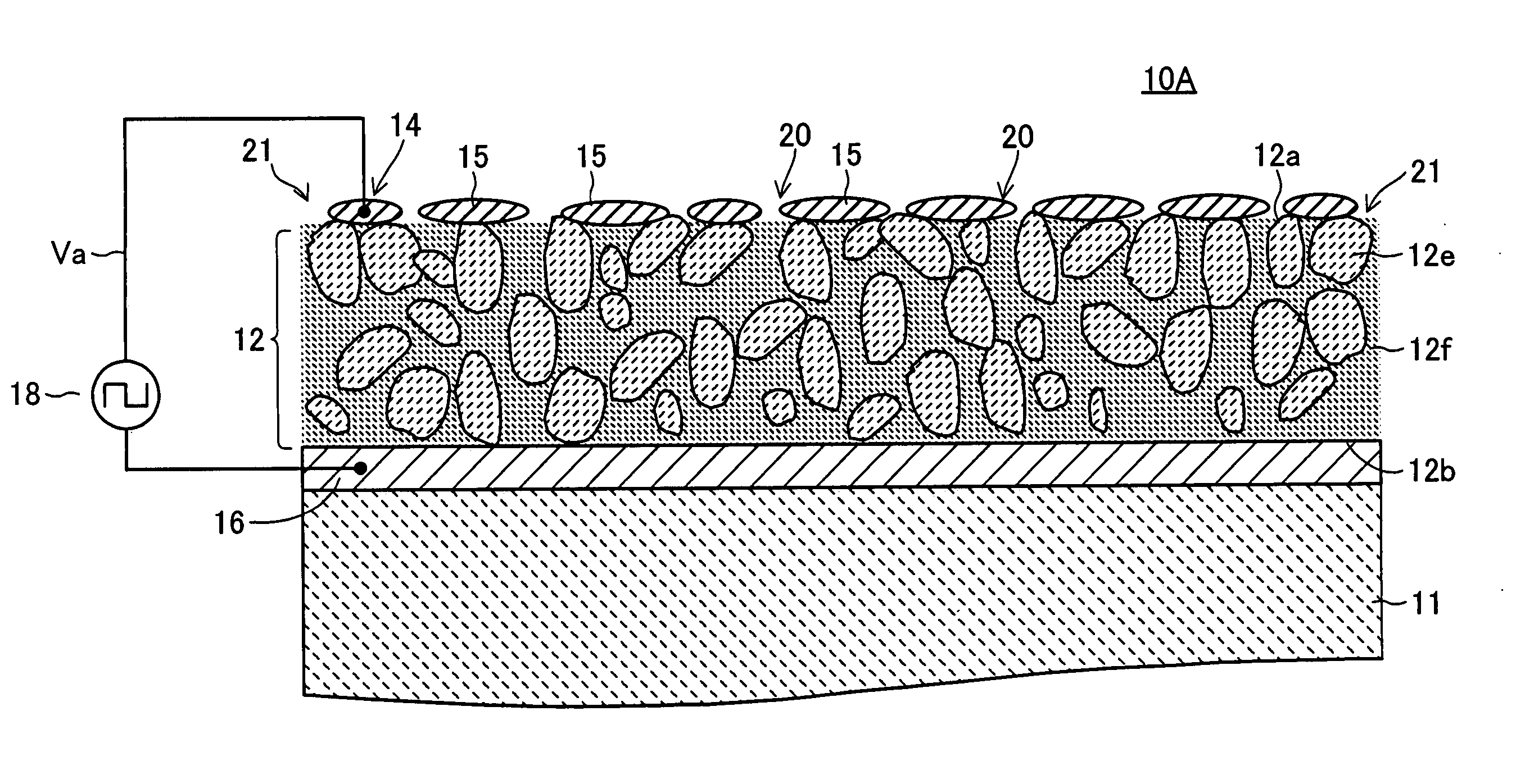
[0086] Firstly, an electron emitter as a dielectric device according to the first embodiment is explained on the basis of FIGS. 1 to 8. FIG. 1 is an enlarged sectional side view of an electron emitter 10A according to the present embodiment. The electron emitters 10A are two-dimensionally formed in large numbers on a glass substrate 11 and one of them is shown in FIG. 1. The electron emitter 10A is provided with: a tabular emitter 12; an upper electrode...


PUM


Abstract

A higher performance dielectric device is provided. An electron emitter applying the dielectric device according to the present invention includes an emitter formed of a dielectric, and an upper electrode and a lower electrode to which a drive voltage is applied to cause electron emission. The emitter includes plural dielectric particles, and plural dielectric particles of smaller particle size which are filled in spaces between the plural dielectric particles. The emitter having the aforesaid construction is formed by an aerosol deposition method or a sol impregnation method.

Description

BACKGROUND OF THE INVENTION [0001] 1. Field of the Invention [0002] This invention relates to a dielectric device using dielectric properties and electrical-mechanical conversion properties. [0003] 2. Description of the Related Art [0004] In the related art, a type of dielectric device using ferroelectric ceramics is known. The dielectric device using this ferroelectric ceramics can usually be obtained by forming a laminated structure, by patterning an electrode on a ferroelectric ceramic thin plate formed by the screen printing method or the green sheet method, or joining to another metal or a ceramic thin plate. [0005] Here, the screen printing method is a method of obtaining a ceramic thin plate used as the base of a dielectric device by forming a film on a predetermined substrate from a slurry containing a ceramic powder dispersed in an organic binder by screen printing, and sintering this film at a high temperature of 900° C. or higher. The green sheet method is a method of obt...

Claims


Application Information

Patent Timeline
Patent Type & Authority Applications(United States)
IPC IPC(8): H01J1/38
CPCB82Y10/00H01J1/312H01J2329/00H01J2201/3125H01J2201/306
Inventor NANATAKI, TSUTOMUYAMAGUCHI, HIROFUMIKOBAYASHI, NOBUYUKI
Owner NGK INSULATORS LTD
Why Eureka
Try Eureka