Light emitting device

Active Publication Date: 2006-01-19
TOYODA GOSEI CO LTD
View PDF18 Cites 275 Cited by
  • Summary
  • Abstract
  • Description
  • Claims
  • Application Information

AI Technical Summary

Benefits of technology

[0043] In the light emitting device thus composed, by equalizing the thermal expansion coefficient of optical element and submount, the stress due to temperature difference between the optical element and the submount can be reduced. Therefore, the stress damage to optical element can be prevented that is caused by process temperature in device fabrication, atmosphere temperature of reflow oven or heat in operation of optical element. Further, by equalizing the thermal expansion coefficient of support member and sealing member, inserting the submount into the penetrating hol

Problems solved by technology

However, the epoxy resin is gradually colored and turns yellow when it is irradiated by intensive light emitted from the LED element.
However, the light emitting device of prior art 1 has the next problems:
The air bubbles once contained therein are difficult to separate.
The residual stress may cause a crack in the glass material when being subjected

Method used


Image

  • Light emitting device
  • Light emitting device
  • Light emitting device

Examples


first embodiment

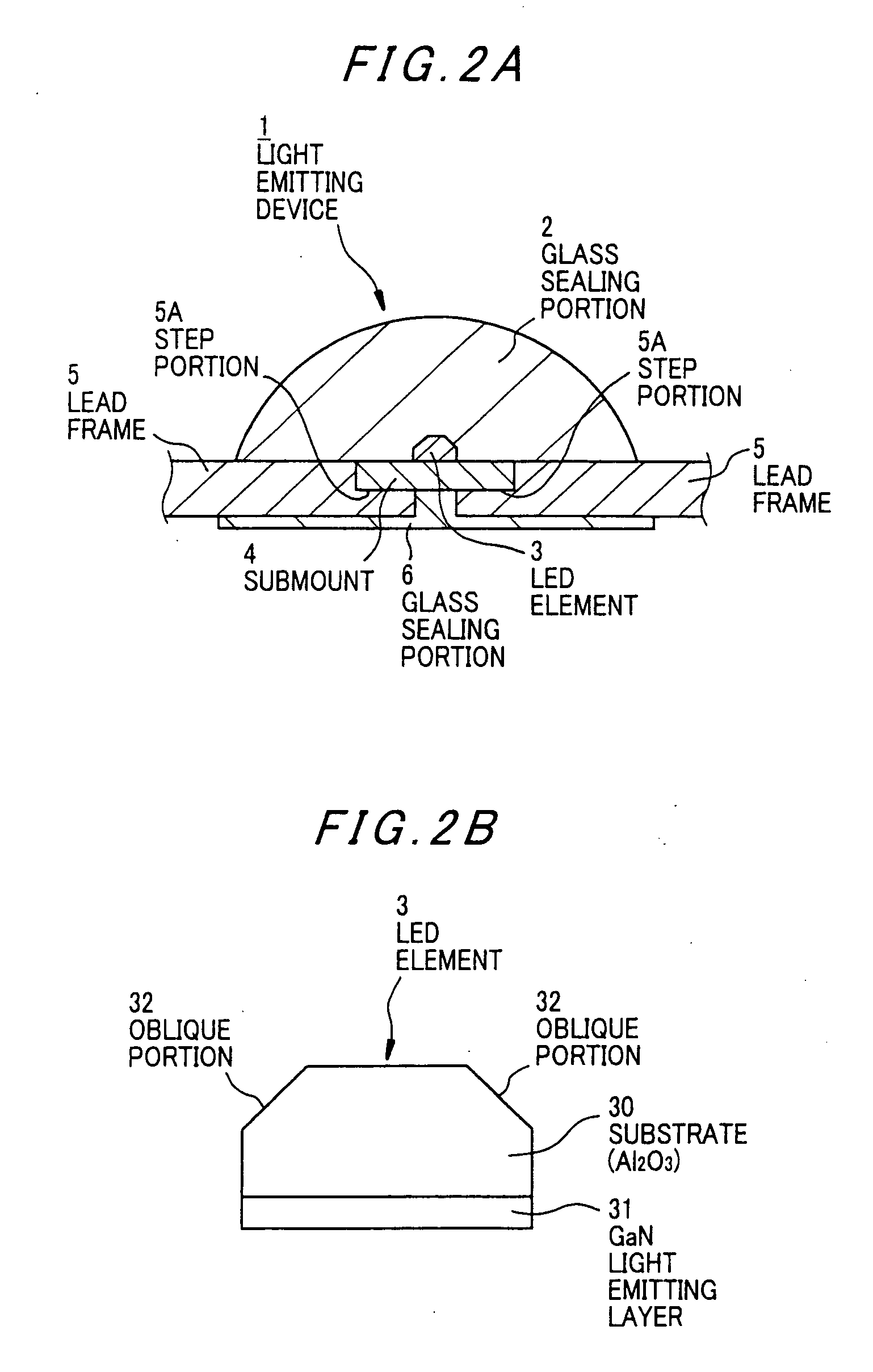
[0103] In the first embodiment, since the corners of LED element 3 are obliquely cut off to offer the oblique portions 32, the turbulence of glass can be reduced when integrally molding the low-melting glass being softened at about 108 to 1010 poises. Thereby, the uniformity of glass can be maintained and the inclusion of air can be prevented. Therefore, the light emitting device 1 with reduced residual bubble can be obtained. Further, because of cutting off the acute corner that the internal stress is likely to concentrate, the occurrence of crack by a heat shock in the glass sealing portion 2 can be prevented. The cutting is easily conducted by using a suitable cutter in the wafer dicing.

[0104] Although in the first embodiment the LED element 3 is provided with the oblique portions 32 at the four corners on the emission observing surface side, edges defined between the emission observing surface and the side face of LED element 3 may be also cut off. Thereby, the residual bubble a...

second embodiment

[0109] In the second embodiment, because of having the curved portions at the corners, the turbulence of glass can be more effectively reduced when integrally molding the softened low-melting glass by hot pressing. Thereby, the residual bubble around the LED element 3 can be further reduced (enhancing the uniformity of glass), and the occurrence of crack can be further prevented.

[0110] In addition to the curved portions 33 at the four corners on the emission observing surface side, edges defined between the emission observing surface and the side face of LED element 3 may be also cut off. Thereby, the residual bubble around the LED element 3 can be further reduced (enhancing the uniformity of glass), and the occurrence of crack can be further prevented.

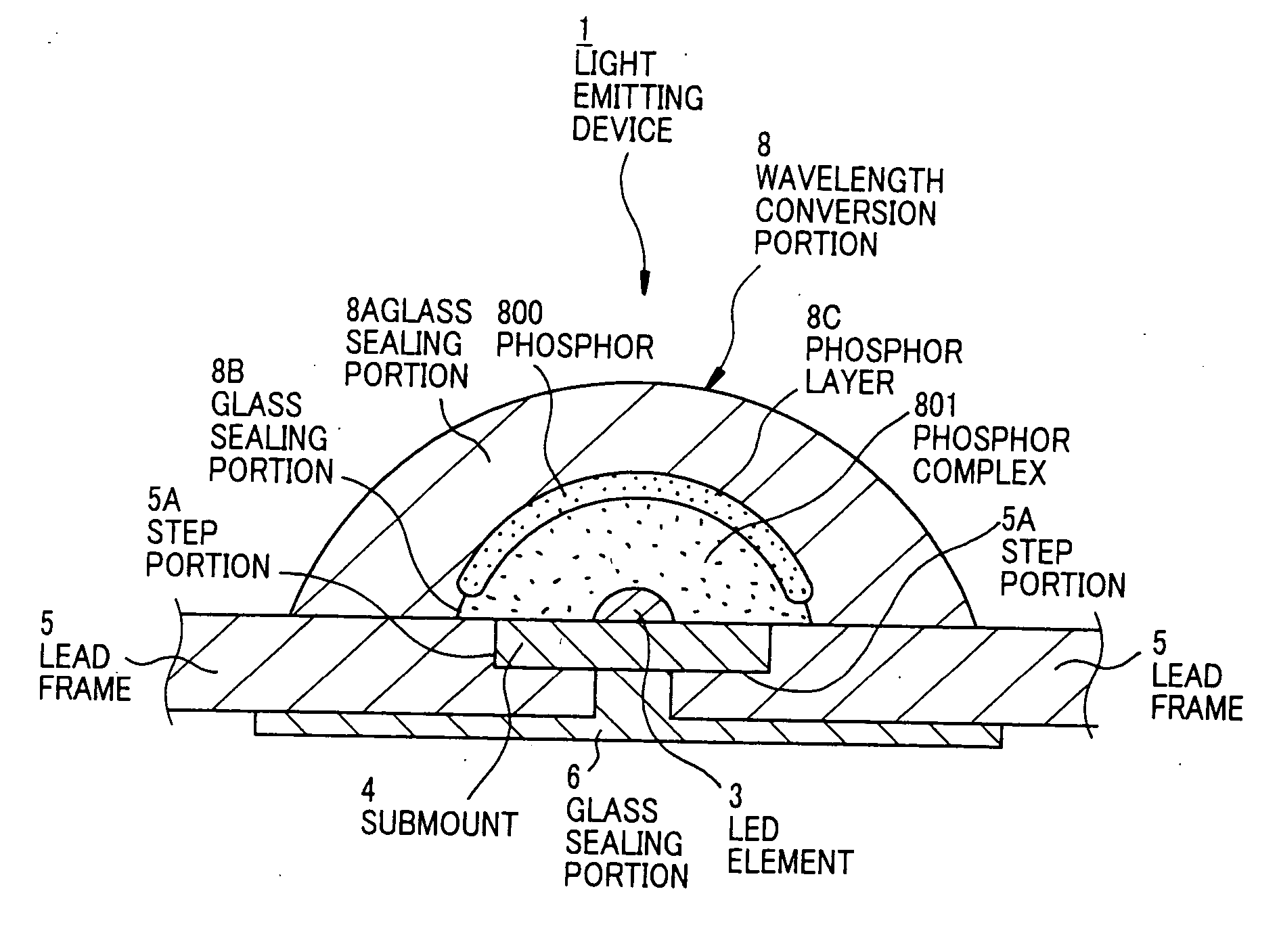
[0111]FIG. 6 is a cross sectional view showing the central portion of a light emitting device in the third preferred embodiment of the invention.

[0112] The light emitting device 1 is constructed as a wavelength conversion device com...

fifth embodiment

[0128] In the fifth embodiment, the substrate 30 of GaN has a big refractive index of n=2.4 and therefore the light extraction efficiency can be enhanced. Light not to be radiated when using the substrate 30 of Al2O3 can be externally radiated from the GaN light emitting layer 31. Further, if the LED element 3 is formed as a rectangular solid, an incident mode exceeding the critical angle to the interface of LED element 3 will be generated. However, the oblique portion 32 formed on the substrate 30 allows the radiation of light from the GaN light emitting layer 31 even in such an incident mode. Thus, loss in light radiation can be reduced.

[0129] The material of substrate 30 is not limited to GaN and may be SiC etc. that has a refractive index similar to that of GaN substrate 30.

[0130]FIG. 9 illustrates a light emitting area and a light radiation of an LED element in the sixth preferred embodiment of the invention.

[0131] As shown, the LED element 3 has a light emitting area A small...


PUM


Abstract

A light emitting device has: a light emitting element; a lead that is electrically connected to the light emitting element at its one end and serves as a terminal to supply a power source to the light emitting element; a metal base that the light emitting element is mounted thereon and radiates heat of the light emitting element; and a sealing member that is of transparent resin or glass and covers the light emitting element. The lead is secured to the metal base by a heat-resisting insulating member with a thermal expansion coefficient nearly equal to that of the metal base.

Description

[0001] The present application is based on Japanese patent application Nos. 2003-276099, 2003-353007 and 2003-358308, the entire contents of which are incorporated herein by reference. BACKGROUND OF THE INVENTION [0002] 1. Field of the Invention [0003] This invention relates to a light emitting device that a light emitting diode (hereinafter referred to as LED) as a light source is sealed with a moisture-impermeable material such as glass. [0004] Also, this invention relates to a light emitting device that heat generated from a high-output light emitting element can be effectively radiated. [0005] 2. Description of the Related Art [0006] Conventionally, light emitting devices using LED as a light source are known. An example thereof is a light emitting device that an LED element is integrally sealed with sealing resin such as epoxy resin. [0007] The epoxy resin is widely available and is easy to mold. Therefore, it is widely used as a sealing material for light emitting device. Howe...

Claims


Application Information

Patent Timeline
IPC IPC(8): H05B33/04H05B33/00H01L33/20H01L33/56H01L33/62H01L33/64
CPCF21K9/00H01L33/20H01L33/56H01L33/62H01L33/642H01L25/0753H01L2224/48247H01L2224/48257Y10S362/80H01L2224/48091H01L2924/00014H01L2924/181H01L2224/8592H01L2924/00012
Inventor SUEHIRO, YOSHINOBUTOHMON, RYOICHIWADA, SATOSHI
Owner TOYODA GOSEI CO LTD
Why Eureka
Try Eureka