Image processing method, semiconductor device for detecting physical quantity distribution, and electronic apparatus

a semiconductor device and physical quantity technology, applied in the field of image processing method, can solve the problems of inability to increase the dynamic range, disadvantageous increase of the system scale, and restricted type of sensor device, and achieve the effect of simple digital processing and increasing the dynamic rang

Inactive Publication Date: 2006-01-19
SONY CORP
View PDF2 Cites 49 Cited by
  • Summary
  • Abstract
  • Description
  • Claims
  • Application Information

AI Technical Summary

Benefits of technology

[0018] In view of the above-described circumstances, it is an object of the present invention to provide a mechanism for increasing the dynamic range with simple digital processing without restricting the type of sensor device.

Problems solved by technology

However, the dynamic range cannot be increased unless a sensor structure having an inter-pixel memory is used.
That is, the type of sensor device is restricted.
Further, since two frames having different accumulation periods are combined by the off-chip method, the system scale is disadvantageously increased.

Method used


Image

  • Image processing method, semiconductor device for detecting physical quantity distribution, and electronic apparatus
  • Image processing method, semiconductor device for detecting physical quantity distribution, and electronic apparatus
  • Image processing method, semiconductor device for detecting physical quantity distribution, and electronic apparatus

Examples


first embodiment

; Signal Difference Processing Operation

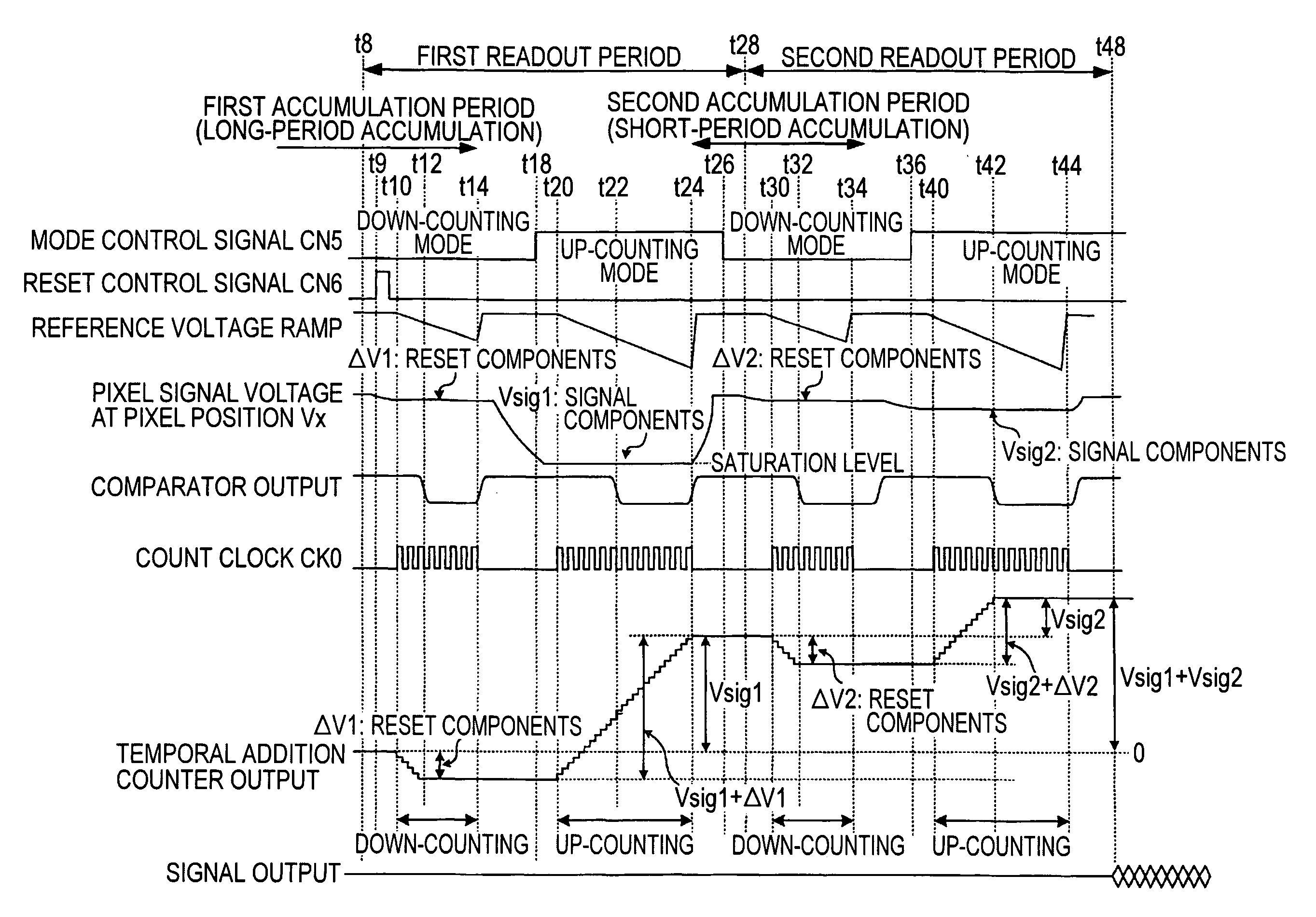
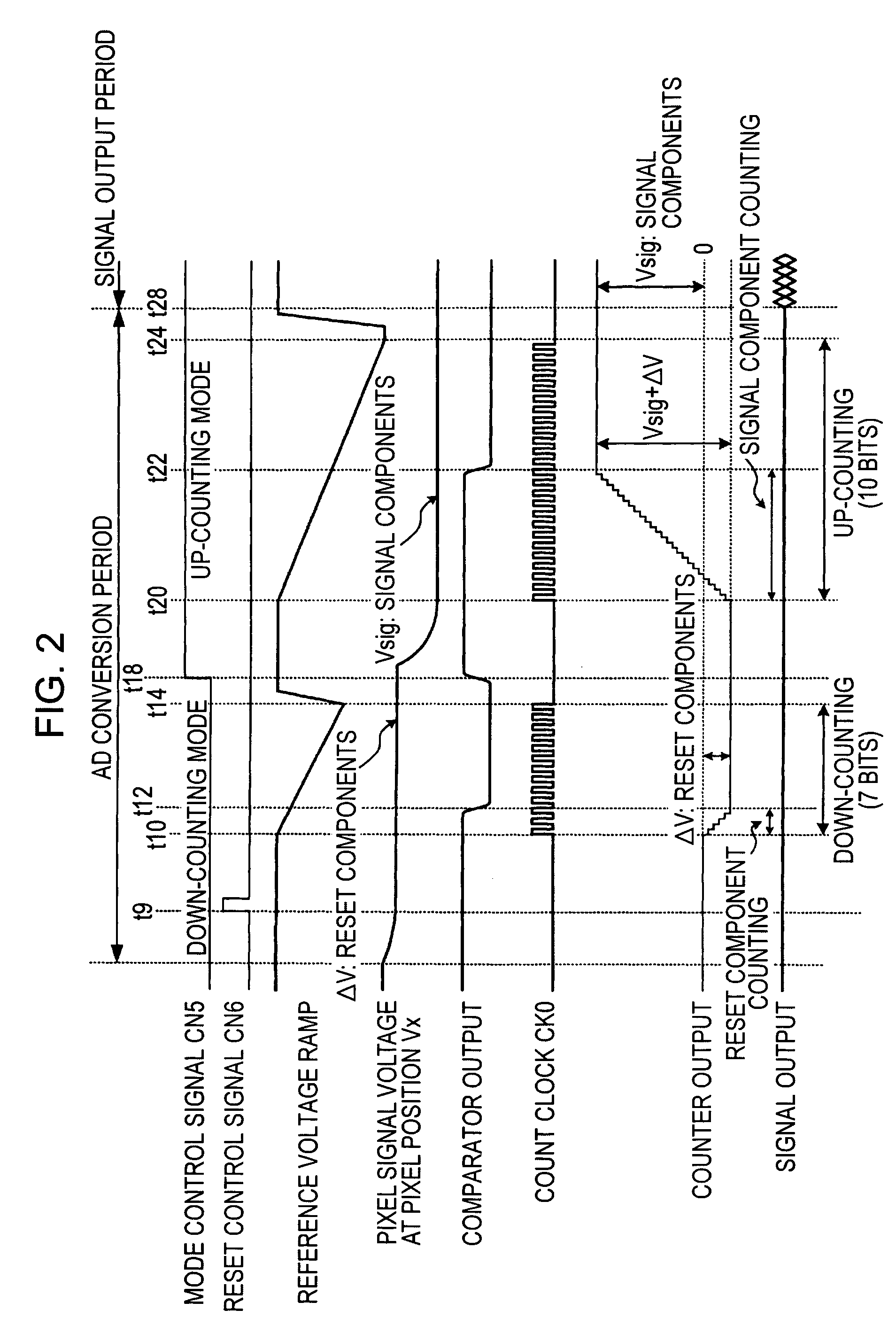
[0113]FIG. 2 is a timing chart illustrating the signal difference processing, which is the basic operation, in the column AD circuit 25 of the solid-state imaging apparatus 1 of the first embodiment shown in FIG. 1.

[0114] The mechanism for converting an analog pixel signal sensed in each pixel unit 3 of the pixel portion 10 into a digital signal is, for example, as follows. The time when the ramp waveform reference signal RAMP which is progressively reduced with a predetermined gradient becomes equal to the voltage of the reference components or the signal components of the pixel signal of the unit pixel 3 is searched, and the time from when the reference signal RAMP used for comparison processing is generated until when the electric signal corresponding to the reference components or the signal components of the pixel signal coincides with the reference signal is counted by the count clock, thereby obtaining the count value associated with t...

second embodiment

; Configuration of Solid-State Imaging Apparatus; Extension of Short Accumulation Period

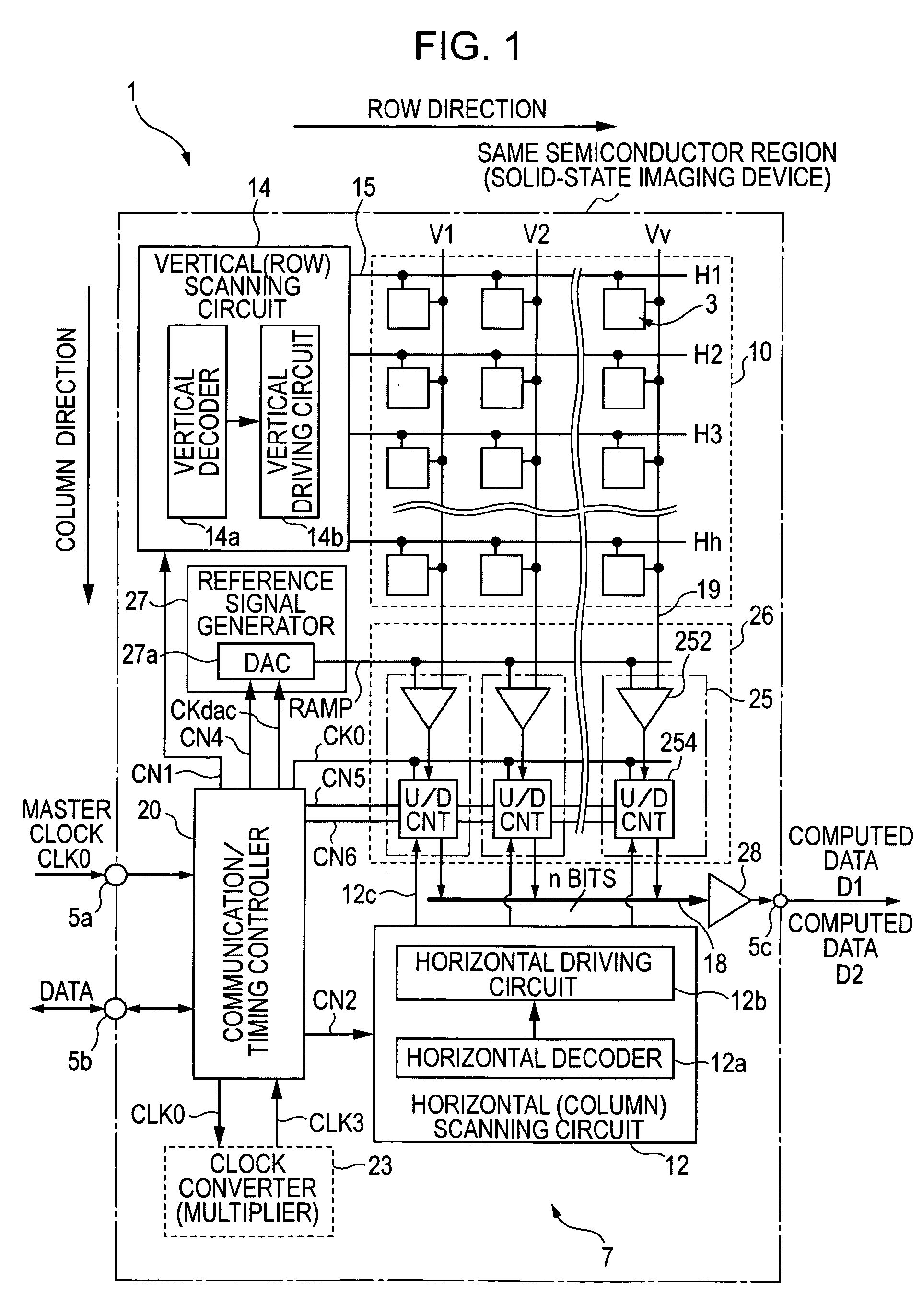
[0182]FIG. 8 is a schematic diagram illustrating a CMOS solid-state imaging apparatus according to a second embodiment of the present invention. FIG. 9 illustrates the relationship between an example of the configuration of the unit pixel 3 and a drive circuit.

[0183] The solid-state imaging apparatus 1 of the second embodiment includes dedicated functions for controlling the long and short accumulation periods (exposure time), independently of the vertical scanning circuit 14, i.e., an accumulation period controller 14A for controlling the long accumulation period and an accumulation period controller 14B for controlling the short accumulation period.

[0184] The unit pixel 3 has a 4TR structure, which is common for CMOS sensors, as shown in FIG. 9. Alternatively, though it is not shown, as disclosed in Patent Number 2708455, the pixel unit 3 having a 3TR, such as an amplifying transistor connect...


PUM


Abstract

An image processing method for obtaining digital data comprising the steps of obtaining a plurality of image signals under a condition of different accumulation periods as an initial value for a counting operation, comparing, by using digital data for a first image signal of the plurality of image signals, an electric signal corresponding to a second image signal of the plurality of image signals with a reference signal, obtaining digital data for the second image signal, performing a counting operation in a mode having the same sign as the sign of digital data for the first image signal between a down-counting mode and an up-counting mode while the comparing step is being performed, and storing a count value.

Description

CROSS PREFERENCE TO RELATED APPLICATIONS [0001] The present claims the benefit of Japanese Patent Application JP 2004-209888 filed in the Japanese Patent Office on Jul. 16, 2004, the entire contents of which are incorporated herein by reference. FIELD OF THE INVENTION [0002] The present invention relates to an image processing method, a semiconductor device for detecting the physical quantity distribution in which a plurality of unit elements are disposed, and an electronic apparatus. More specifically, the invention relates to a digital signal processing technology suitably used for semiconductor devices for detecting the physical quantity distribution, for example, solid-state imaging apparatuses, and other electronic apparatuses, in which a plurality of unit elements responsive to electromagnetic waves, such as light or radiation, input from an external source, are disposed, and the physical quantity distribution obtained by converting electromagnetic waves into an electric signa...

Claims


Application Information

Patent Timeline
Patent Type & Authority Applications(United States)
IPC IPC(8): H03M1/12G03G15/10G06K9/32H03M1/48H04N5/335H04N5/355H04N5/374H04N5/378
CPCH04N5/335H04N25/00H04N25/57H04N25/77
Inventor NITTA, YOSHIKAZUFUKUSHIMA, NORIYUKIMURAMATSU, YOSHINORIYASUI, YUKIHIRO
Owner SONY CORP
Why Eureka
Try Eureka