
Plasma treatment apparatus and light detection method of a plasma treatment

Inactive Publication Date: 2006-01-19
VERITY INSTR +1
View PDF16 Cites 11 Cited by
  • Summary
  • Abstract
  • Description
  • Claims
  • Application Information

AI Technical Summary

Benefits of technology

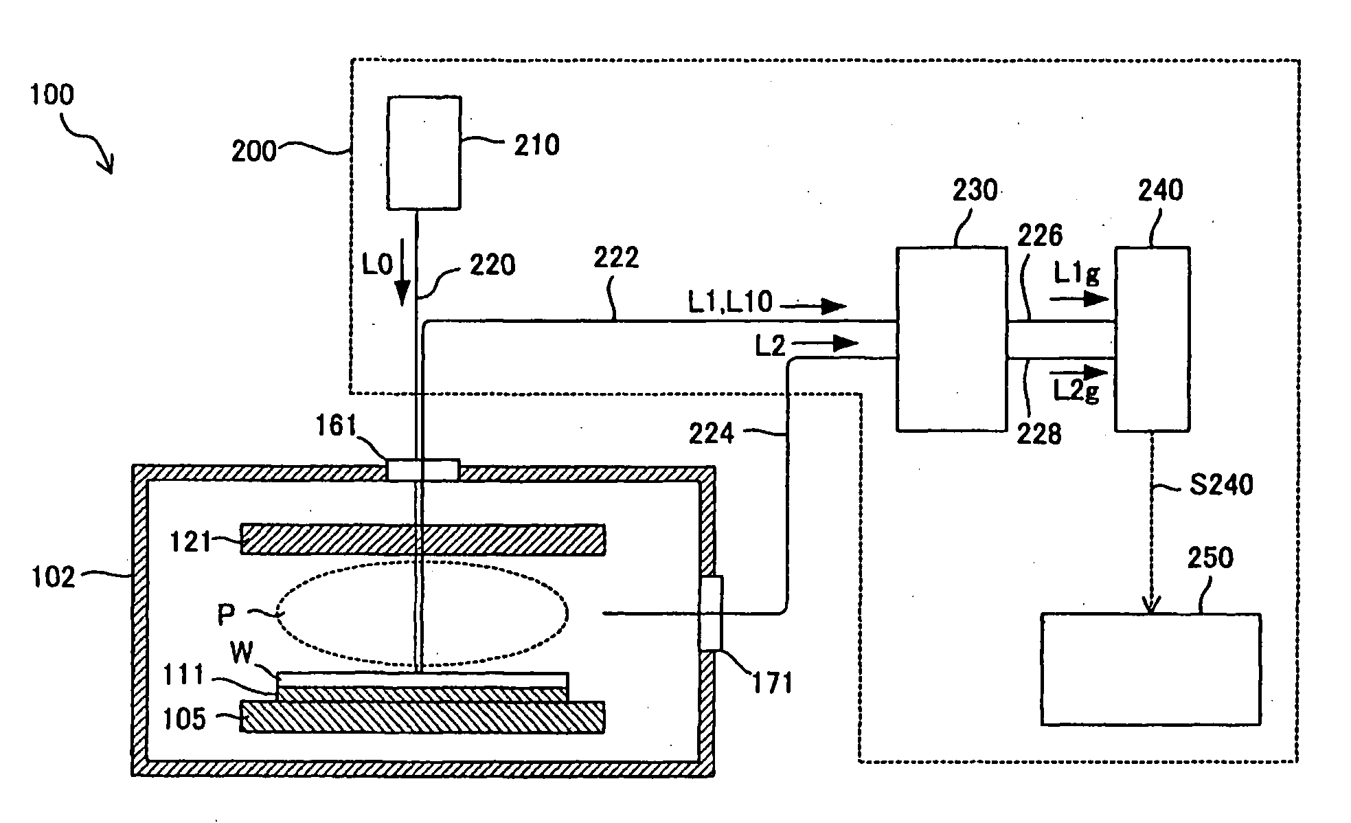
[0014] According to the plasma treatment apparatus having this structure, the photoelectric conversion element region having the interference light photoreception region and the plasma light photoreception region receives interference light and plasma light. Thus there is no need for preparation of separate respective photoelectric conversion components for interference light and for plasma light. This results in a size reduction of the plasma treatment apparatus.
[0015] Moreover, the above mentioned photoelectric conversion component has an electric charge storage member for storing electrical charge transmitted from the photoelectric conversion element region. The electric charge generated by those photoelectric conversion elements belonging to the interference light photoreception region is transmitted to the electric charge storage member through the plasma light photoreception region. Due to this structure, electric charge generated by photoelectric conversion elements belonging to the interference light photoreception region does not require securing a separate path for transmission to the electric charge storage member, and this results in a size reduction of the plasma treatment apparatus.
[0017] The above mentioned photoelectric conversion element region preferably has a light-shielded region that overlaps neither the interference light photoreception region nor the plasma light photoreception region. By sending the photoelectric-converted electrical charge group to the light-shielded region from the interference light photoreception region and plasma light photoreception region, it becomes possible to continuously receive interference light in the interference light photoreception region, and it becomes possible to continuously receive plasma light in the plasma light photoreception region. Moreover, since external light does not strike the light-shielded region, it is possible to maintain electrical charge groups sent from the interference light photoreception region and the plasma light photoreception region in a stabilized state.
[0019] According to this light detection method, it becomes possible to detect interference light and plasma light by a single photoelectric conversion component without provision of separate respective photoelectric conversion components for the interference light and the plasma light, and this results in a size reduction of the plasma treatment apparatus.
[0020] Furthermore, the electrical charge group obtained by photoelectric conversion of plasma light is sent to the electrical charge storage member from the plasma light photoreception region, and the electrical charge group obtained from the interference light is preferably sent to the electrical charge storage member through the plasma light photoreception region from the interference light photoreception region. The electrical charge group generated by photoelectric conversion elements belonging to the interference light photoreception region is sent to the electrical charge storage member without the need for securing a separate route, and this results in a size reduction of the photoelectric conversion component.

Problems solved by technology

As a result, scale of the treatment apparatus increases, the space occupied by the treatment apparatus must be increased, and the cost of the treatment apparatus is increased.

Method used


Image

  • Plasma treatment apparatus and light detection method of a plasma treatment
  • Plasma treatment apparatus and light detection method of a plasma treatment
  • Plasma treatment apparatus and light detection method of a plasma treatment

Examples


working examples

[0036] Preferred embodiments of the plasma treatment apparatus and the plasma treatment apparatus light detection method according to the present invention are explained below while referring to the appended figures. Furthermore, within the present specification document and the figures, constituent elements having substantially the same mechanical structure are assigned the same identifying number, and redundant explanations are omitted.

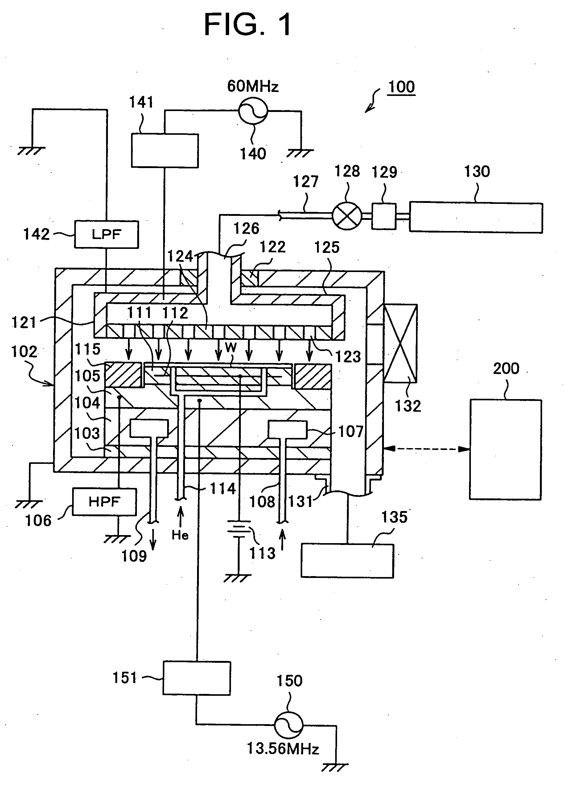
[0037] Structure of an etching apparatus 100, as a plasma treatment apparatus that is a working example of the present invention, is explained while referring to figures. FIG. 1 is a cross-sectional schematic drawing showing structure of etching apparatus 100. Etching apparatus 100 is constructed as a capacitively-coupled flat-plate etching apparatus having upper and lower parallel opposing electrodes for which one electrode contacts the power source used for plasma formation.

[0038] This etching apparatus 100 has a treatment chamber (chamber) 102 ...


PUM


Abstract

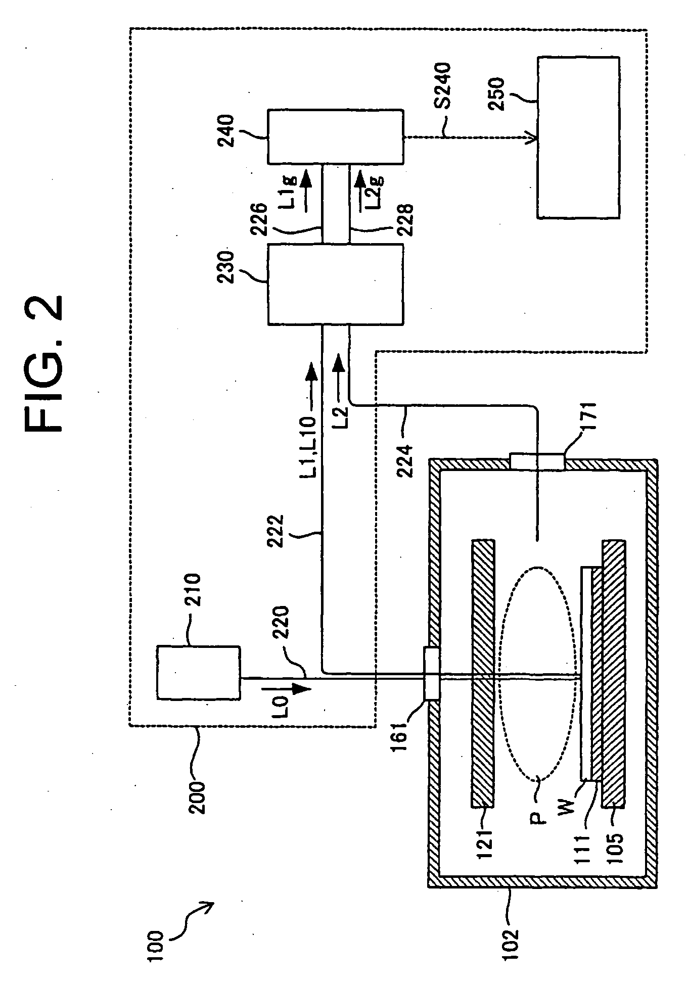
The subject of the invention is a plasma treatment apparatus and light detection method capable of detecting multiple optical signals obtained from multiple measurement locations and capable of analyzing condition of each of the measurement locations using an apparatus having the advantage of having a more simplified structure. Interference light L1 passes through optical fiber 222 and is transmitted to spectroscopic component 230. Plasma light L2 passes through optical fiber 224 and is transmitted to spectroscopic component 230. These lights separately undergo respective spectroscopic separation. Interference light spectrum L1g obtained by spectroscopic separation of interference light L1 passes through first light path 226 and strikes an interference light photoreception region of photoelectric conversion component 240. Plasma light spectrum L2g obtained by spectroscopic separation of plasma light L2 passes through second light path 228 and strikes a plasma light photoreception region of photoelectric conversion component 240.

Description

BACKGROUND OF THE INVENTION [0001] 1. Technical Field Relating to the Invention [0002] The present invention relates to a plasma treatment apparatus and a light detection method of a plasma treatment apparatus. [0003] 2. Conventional Technology [0004] Etching treatment by plasma is widely used for the production processes of semiconductor devices and LCD (Liquid Crystal Display) substrates. The treatment apparatus utilized for this plasma treatment, for example, is equipped with an upper electrode and a lower electrode disposed parallel to one another. While the treatment workpiece (e.g. a semiconductor wafer) is carried and held on the lower electrode, plasma is generated between the upper electrode and the lower electrode. The treatment workpiece is subjected to etching of a certain pattern by this plasma. [0005] Scale of the holes and trenches formed by plasma treatment is currently being reduced. This requires real-time observation of the treatment apparatus operating state and ...

Claims


Application Information

Patent Timeline
IPC IPC(8): G01B9/02
CPCH01J37/32972G01N21/68
Inventor SAITO, SUSUMUKUENY, ANDREW WEEKS
Owner VERITY INSTR
Learn More