Developable phosphor coating mixture solution and method for manufacturing anodic phosphor layer

a technology of phosphor coating and mixture solution, which is applied in the direction of electrostatic spraying apparatus, coating, bleaching apparatus, etc., can solve the problem that the silkscreen printing method cannot produce high-resolution graphics, and achieve the effect of increasing the adhesion strength

Inactive Publication Date: 2006-01-19
TECO NANOTECH CO LTD
View PDF11 Cites 1 Cited by
  • Summary
  • Abstract
  • Description
  • Claims
  • Application Information

AI Technical Summary

Benefits of technology

[0013] The third purpose of this invention is to provide a developable phosphor coating mixture solution ...

Problems solved by technology

Conventionally, the traditional spin deposition of an anodic phosphor layer on FED is difficult f...

Method used


Image

  • Developable phosphor coating mixture solution and method for manufacturing anodic phosphor layer
  • Developable phosphor coating mixture solution and method for manufacturing anodic phosphor layer

Examples


Embodiment Construction

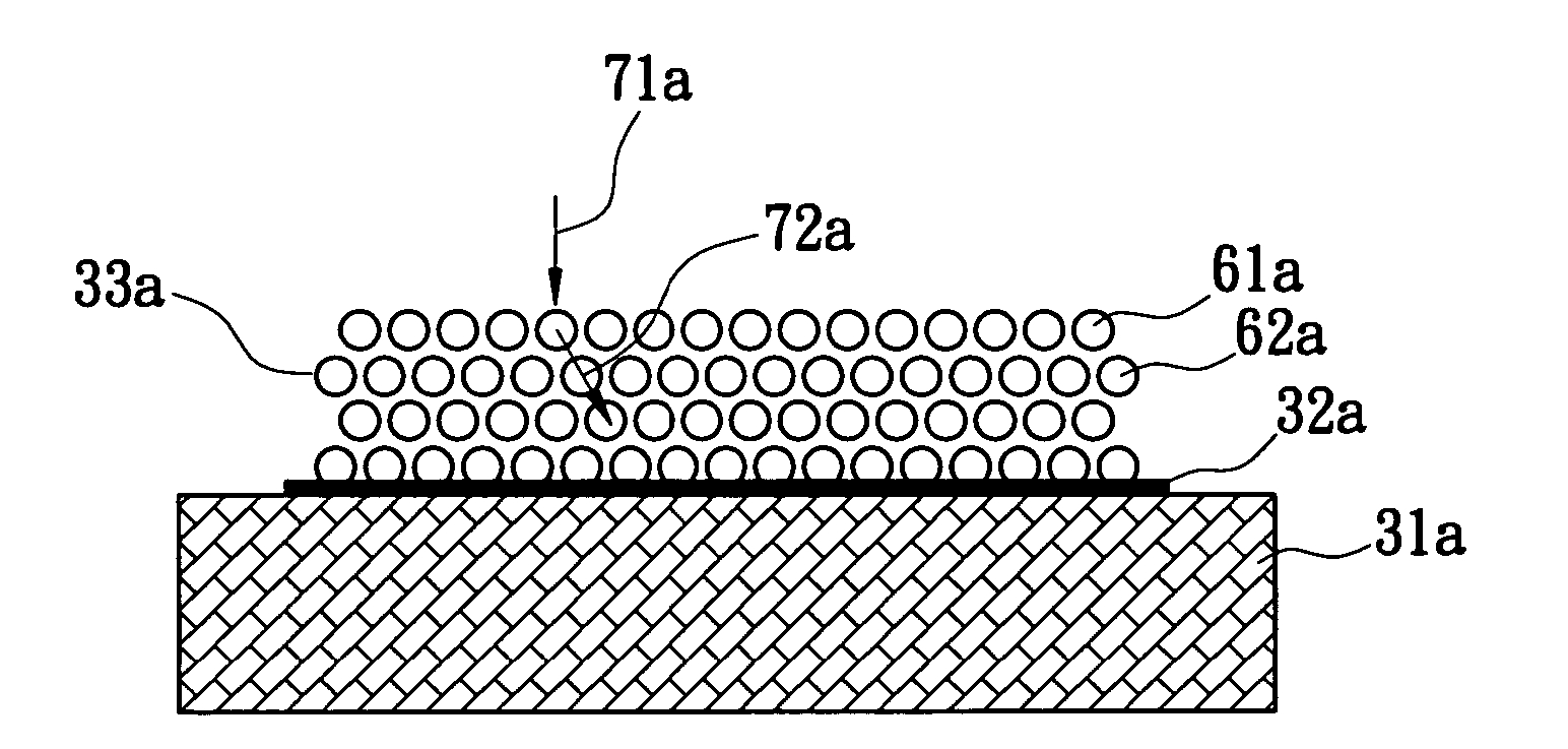
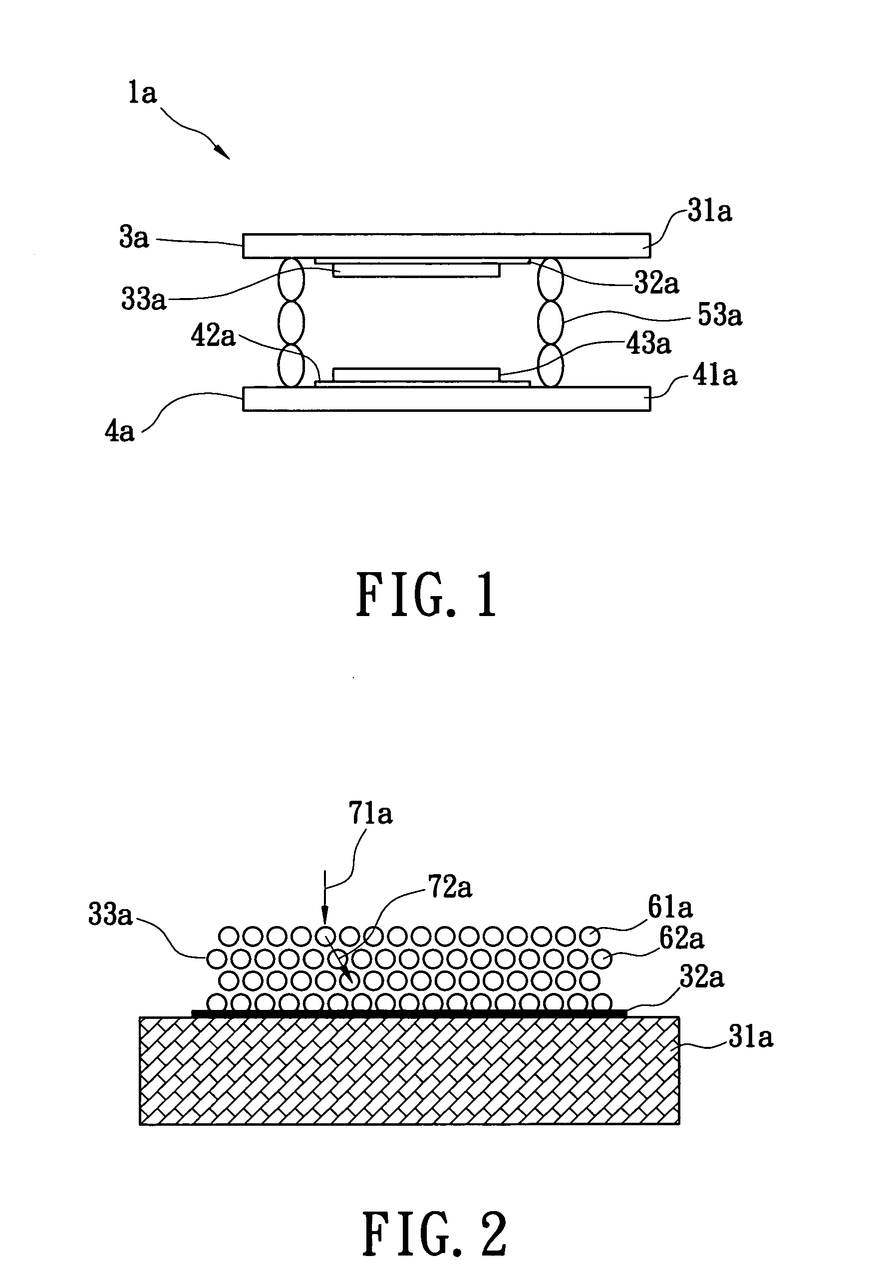
[0022] The present invention provides a printable developable phosphor coating mixture solution for manufacturing a phosphor layer by means of a printing and exposure procedures. The solution is an aqua-resin reacting with an additive photoreaction initialization agent such as dichromate to form a light-negative-resistance solvent. Solvent is then added to phosphor powder, adhesive powder, coagulator and additional conductive power to form a compound solution. The aqua-resin is, for example, aqua-polyvinyl alcohol; the adhesive powder is, for example, glass powder; the coagulator is, for example, silicon dioxide solution of [TEOS; and an additional conductive power is, for example, aluminum powder, indium oxide, or ITO (a semiconductor material, belongs to P-22 series) used to reduce the conductive resistance of the phosphor layer. The compound solution has a high viscosity of over 50000 cps for better usage in the printing process.

[0023] The implementation method comprises the fol...


PUM


Abstract

A developable phosphor coating mixture solution and its manufacturing technique on anodic phosphor layers are described. The anodic phosphor layer of the field emission display is achieved through a silkscreen-printing method copulated with exposure procedure. The process is a simple silkscreen-printing method on an anodic glass substrate. Material features are combined with the manufacturing process to increase the adhesion ability of the phosphor powder on the anodic laminate. The exposure procedure develops high-resolution photography. The simple process and low cost coating can be used in manufacturing glass substrates.

Description

BACKGROUND OF THE INVENTION [0001] 1. Field of the Invention [0002] The present invention relates to a manufacturing technique of a phosphor layer on an anodic laminate of a field emission display (FED), and particularly relates to a manufacturing technique of a patterned phosphor layer by means of a silkscreen-printing copulated with an exposure procedure. [0003] 2. Background of the Invention [0004] Generally, field emission displays (FEDs) are display devices where electrons are liberated from an emitter on a cathode by quantum mechanical tunneling and impinge upon phosphors on an anode, thereby producing a predetermined screen image. [0005] Referring to FIG. 1, a conventional FED 1a includes an anode 3a, a cathode 4a and a rib 53a arranged between the anode 3a and the cathode 4a for forming a vacuum space. As diagram 1 depicts, the anode 3a is constructed by an anodic glass substrate 31a, an anodic electric-conductive layer 32a and a phosphor layer 33a. The cathode 4a is constru...

Claims


Application Information

Patent Timeline
IPC IPC(8): B05D5/06C09K11/02
CPCC09K11/02C09K11/08
Inventor HSIAO, SHIH-CHIENCHENG, KUEI-WENWU, JIA-HUNG
Owner TECO NANOTECH CO LTD
Why Eureka
Try Eureka