Methods of forming a thin film structure, and a gate structure and a capacitor including the thin film structure

a technology of gate structure and capacitor, which is applied in the direction of coating, chemical vapor deposition coating, semiconductor devices, etc., can solve the problems of affecting the reactivity of the semiconductor device, the thickness of the hafnium silicon oxide layer may not have the desired electrical characteristics, and the leakage current may rapidly increase in the semiconductor device including the hafnium oxide layer, etc., to achieve good reactivity, high dielectric constant, and easy formation

Inactive Publication Date: 2006-01-19
SAMSUNG ELECTRONICS CO LTD
View PDF5 Cites 395 Cited by
  • Summary
  • Abstract
  • Description
  • Claims
  • Application Information

AI Technical Summary

Benefits of technology

[0025] According some embodiments of the present invention, a thin film structure including hafnium silicon oxide may be relatively easily formed using TEMAH and APTES both of which have good reactivity with respect to each other. Particularly, the thin film structure may have a desired concentration ratio between hafnium and silicon by controlling the numbers of the cycles of the manufacturing processes in the formation of the thin film structure using an ALD process. Because the thin film structure has a relatively high dielectric constant, a semiconductor device that includes a transistor or a capacitor, for example, may have improved electrical characteristics when the thin film structure is used for a gate insulation layer of the transistor or a dielectric layer of the capacitor.

Problems solved by technology

Because the hafnium oxide layer may be crystallized at a temperature of above about 300° C., however, a leakage current may rapidly increase in a semiconductor device including the hafnium oxide layer.
According to the conventional method of forming a hafnium silicon oxide layer, the hafnium silicon oxide layer may not have desired thickness and electrical characteristics because a hafnium precursor may not easily react with a silicon precursor.
That is, the silicon precursor may not have good reactivity relative to the hafnium precursor so that the hafnium silicon oxide layer may have an undesired thickness or poor electrical characteristics.

Method used


Image

  • Methods of forming a thin film structure, and a gate structure and a capacitor including the thin film structure
  • Methods of forming a thin film structure, and a gate structure and a capacitor including the thin film structure
  • Methods of forming a thin film structure, and a gate structure and a capacitor including the thin film structure

Examples


Embodiment Construction

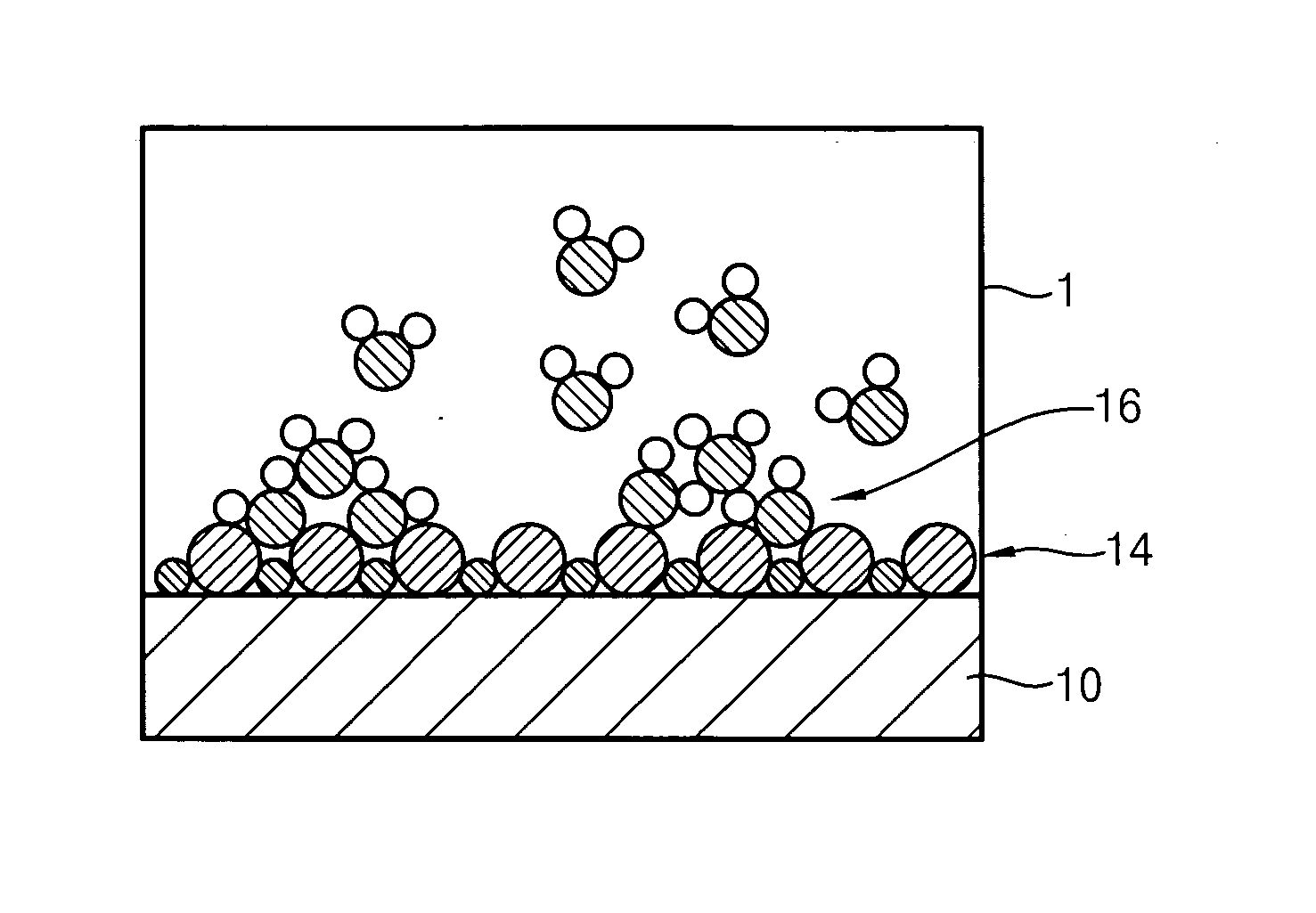
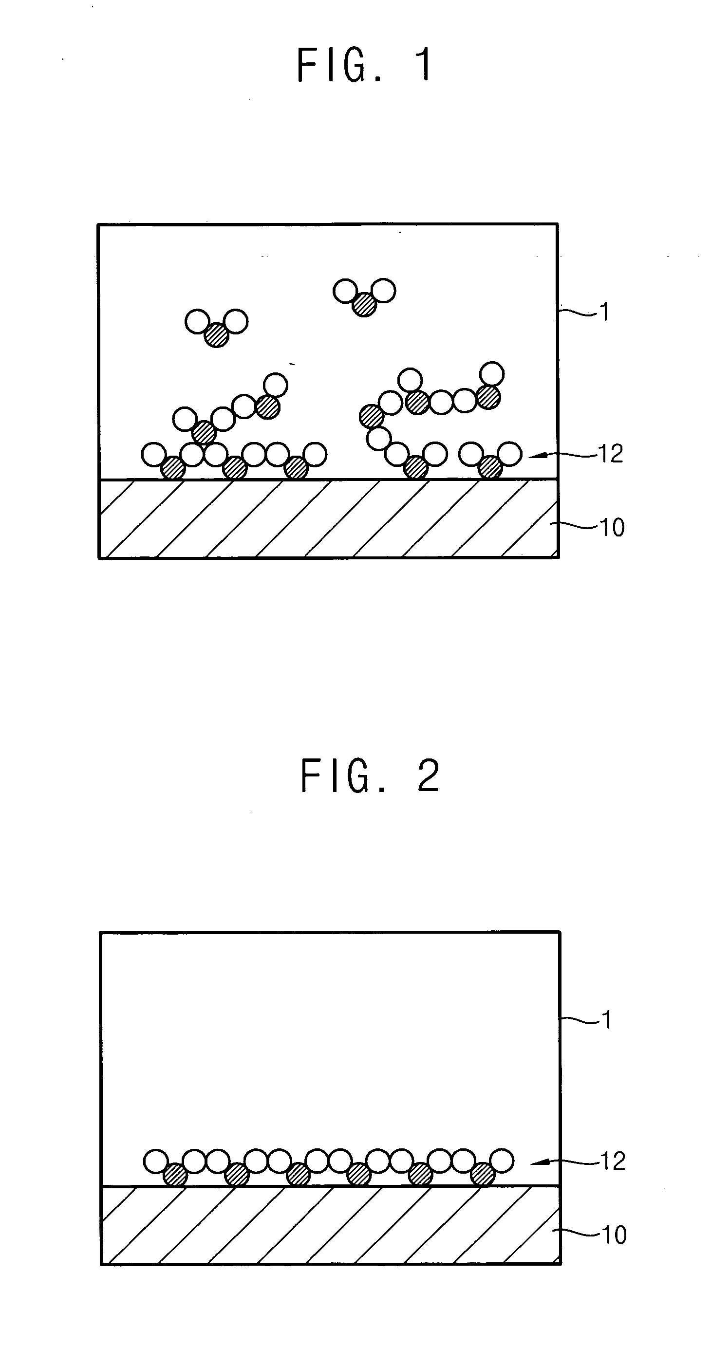
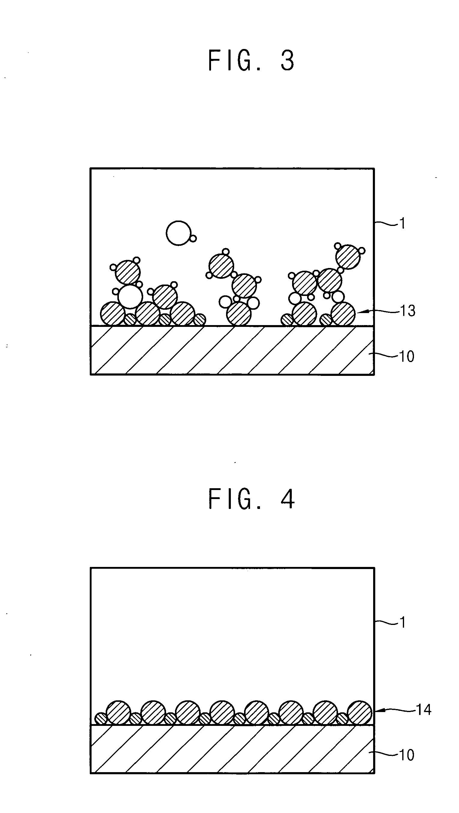
[0034] The invention now will be described more fully hereinafter with reference to the accompanying drawings, in which embodiments of the invention are shown. This invention may, however, be embodied in many different forms and should not be construed as limited to the embodiments set forth herein. Rather, these embodiments are provided so that this disclosure will be thorough and complete, and will fully convey the scope of the invention to those skilled in the art. Like reference numerals refer to like elements throughout the description of the figures.

[0035] It will be understood that when an element is referred to as being “on” another element, it can be directly on the other element or intervening elements may be present. In contrast, when an element is referred to as being “directly on” another element, there are no intervening elements present. As used herein, the term “and / or” includes any and all combinations of one or more of the associated listed items.

[0036] It will b...


PUM

PropertyMeasurementUnit
temperatureaaaaaaaaaa

Abstract

A thin film structure is formed that includes hafnium silicon oxide using an atomic layer deposition process. A first reactant including tetrakis ethyl methyl amino hafnium (TEMAH) is introduced onto a substrate. A first portion of the first reactant is chemisorbed to the substrate, whereas a second portion of the first reactant is physorbed to the first portion of the first reactant. A first oxidant is provided onto the substrate. A first thin film including hafnium oxide is formed on the substrate by chemically reacting the first oxidant with the first portion of the first reactant. A second reactant including amino propyl tri ethoxy silane (APTES) is introduced onto the first thin film. A first portion of the second reactant is chemisorbed to the first thin film, whereas a second portion of the second reactant is physorbed to the first portion of the second reactant. A second oxidant is provided onto the first thin film. A second thin film including silicon oxide is formed on the first thin film by chemically reacting the second oxidant with the first portion of the second reactant.

Description

CROSS REFERENCE TO RELATED APPLICATION [0001] This application claims the benefit under 35 USC § 119 of Korean Patent Application No. 2004-55057 filed on Jul. 15, 2004 the disclosure of which is hereby incorporated herein by reference in its entirety. BACKGROUND OF THE INVENTION [0002] 1. Field of the Invention [0003] The present invention relates to methods of forming a thin film structure using an atomic layer deposition (ALD) process, methods of forming a gate structure including the thin film structure, and methods of forming a capacitor including the thin film structure. More particularly, the present invention relates to methods of forming a thin film structure including hafnium silicon oxide using an ALD process, methods of forming a gate structure including the thin film structure, and methods of forming a capacitor including the thin film structure. [0004] 2. Description of Related Art [0005] A material having a higher dielectric constant may be widely used for a gate insul...

Claims


Application Information

Patent Timeline
Patent Type & Authority Applications(United States)
IPC IPC(8): C23C16/00B05D5/12
CPCC23C16/401C23C16/45531C23C16/45553H01L29/517H01L21/3141H01L21/31616H01L21/31645H01L21/28194H01L21/02148H01L21/0228H01L21/20H01L21/18H10B99/00
Inventor PARK, HONG-BAEKANG, SANG-BOMJIN, BEOM-JUNSHIN, YU-GYUN
Owner SAMSUNG ELECTRONICS CO LTD
Why Eureka
Try Eureka