Low leakage MOS transistor
- Summary
- Abstract
- Description
- Claims
- Application Information
AI Technical Summary
Benefits of technology
Problems solved by technology
Method used
Image

Examples
Embodiment Construction
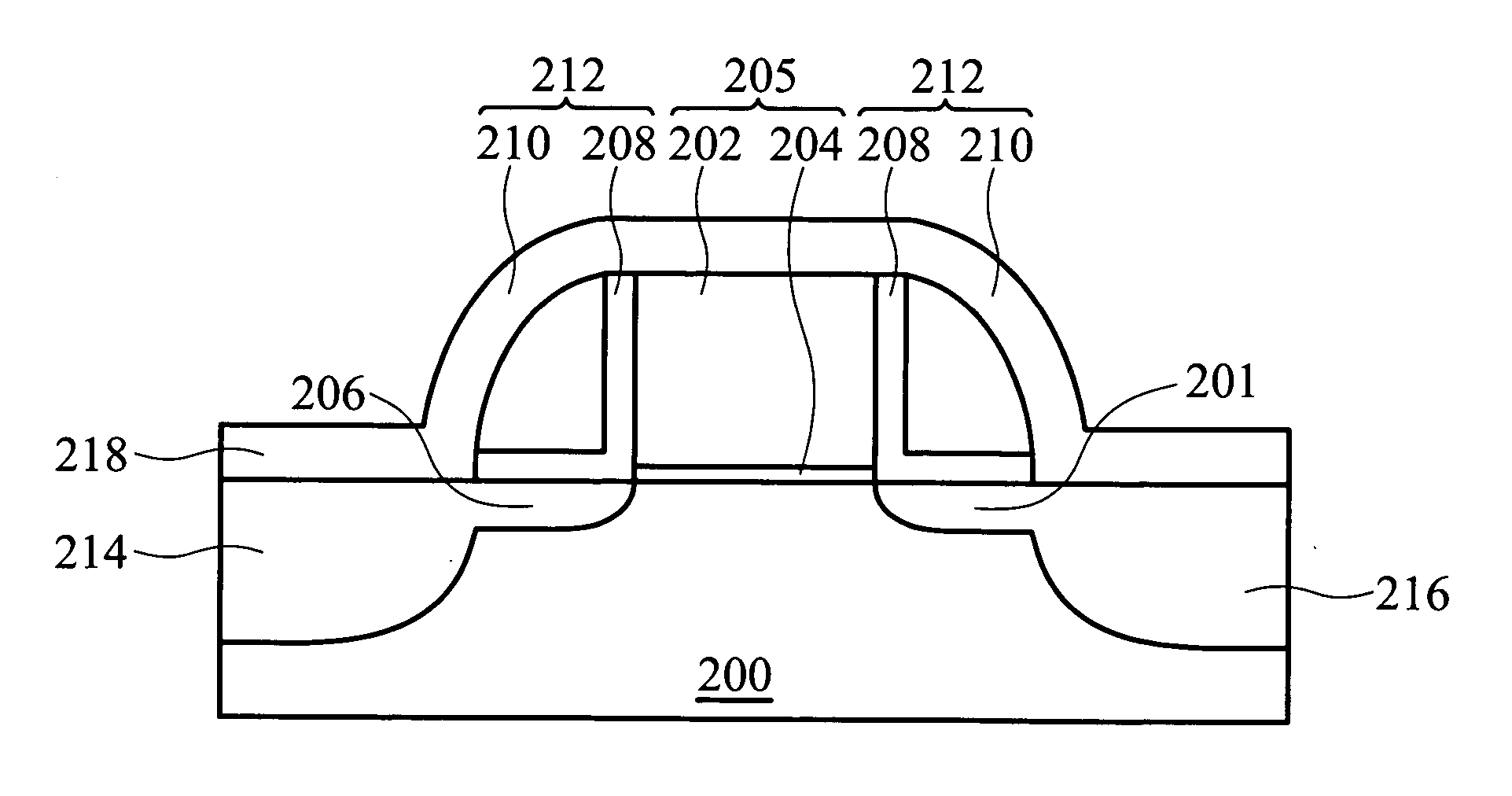
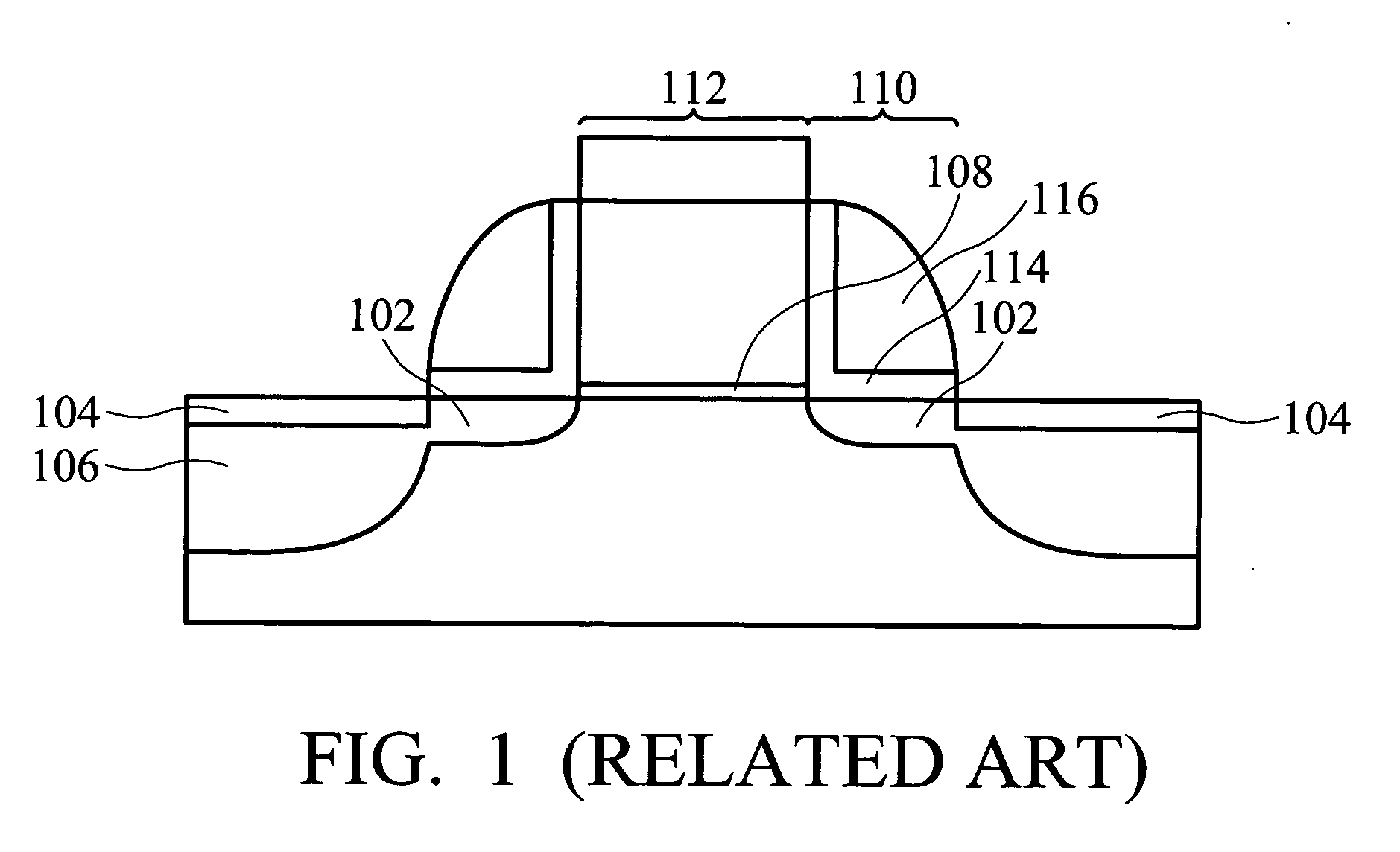
[0017] The present invention, which provides a fabricating method and structure of a low leakage MOS transistor, is described in greater detail by referring to the drawings that accompany the present invention. It is noted that in the accompanying drawings, like and / or corresponding elements are referred to by like reference numerals.
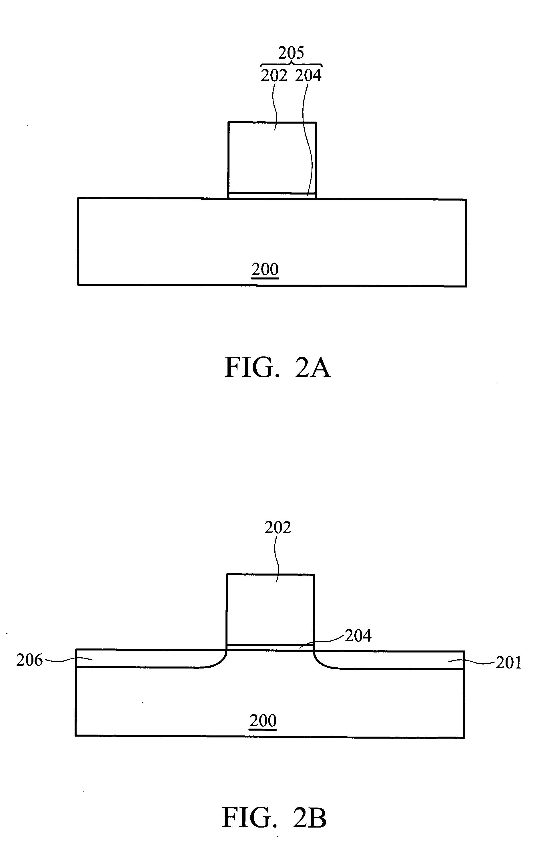
[0018] A method of manufacturing a low leakage MOS transistor is described with reference to FIG. 2A to FIG. 2F.
[0019] As shown in FIG. 2A, a substrate 200 is provided, and a gate dielectric layer 204 and a gate conductive layer 202 are formed thereon. The substrate 200 can be a semiconductor comprising, for example, a semiconductor material such as Si, Ge, SiGe, GaAs, InAs, InP, Si / Si, Si / SiGe, and silicon-on-insulators. The gate conductive layer 202 can be poly silicon or metal, such as W or Ti, and the gate dielectric layer 204 silicon oxide or any high k dielectric material. The substrate 200 can be n-type or p-type, preferably, p-type. The gate c...
PUM
 Abstract
Description
Claims
Application Information
 - R&D Engineer
- R&D Manager
- IP Professional
- Industry Leading Data Capabilities
- Powerful AI technology
- Patent DNA Extraction
Browse by: Latest US Patents, China's latest patents, Technical Efficacy Thesaurus, Application Domain, Technology Topic.
© 2024 PatSnap. All rights reserved.Legal|Privacy policy|Modern Slavery Act Transparency Statement|Sitemap