Ion implanter and method of manufacturing semiconductor device

a semiconductor device and implanter technology, applied in the field of implanter and semiconductor device manufacturing method, can solve the problems of not necessarily eliminated asymmetry of transistor characteristics

Inactive Publication Date: 2006-01-26
KK TOSHIBA
View PDF11 Cites 9 Cited by
  • Summary
  • Abstract
  • Description
  • Claims
  • Application Information

AI Technical Summary

Benefits of technology

[0011] An ion implanter according to an aspect of the present invention comprises a sample stage for setting a sample having a main surface; an ion generating section which generates a plurality of ions, the ion generating section including a container into which an ion source gas is introduced and a filament for emitting thermal electrons provided in the container; an implanting section which implants an ion beam containing the plurality of ions in the main surface of the sample; and a control section which controlles a position of the sample or a spatial distribution of electrons emitted from the filament so that a direction of eccentricity of a center of gravity of the ion beam coincides with a direction of a normal line of the main surface.

Problems solved by technology

A cone angle has been considered to be the cause of the asymmetry of the transistor characteristics which may occur if a batch type high current ion implanter is used.
However, at present, the asymmetry of the transistor characteristics is not necessarily eliminated simply by adjusting the α and β angles.

Method used


Image

  • Ion implanter and method of manufacturing semiconductor device
  • Ion implanter and method of manufacturing semiconductor device
  • Ion implanter and method of manufacturing semiconductor device

Examples


first embodiment

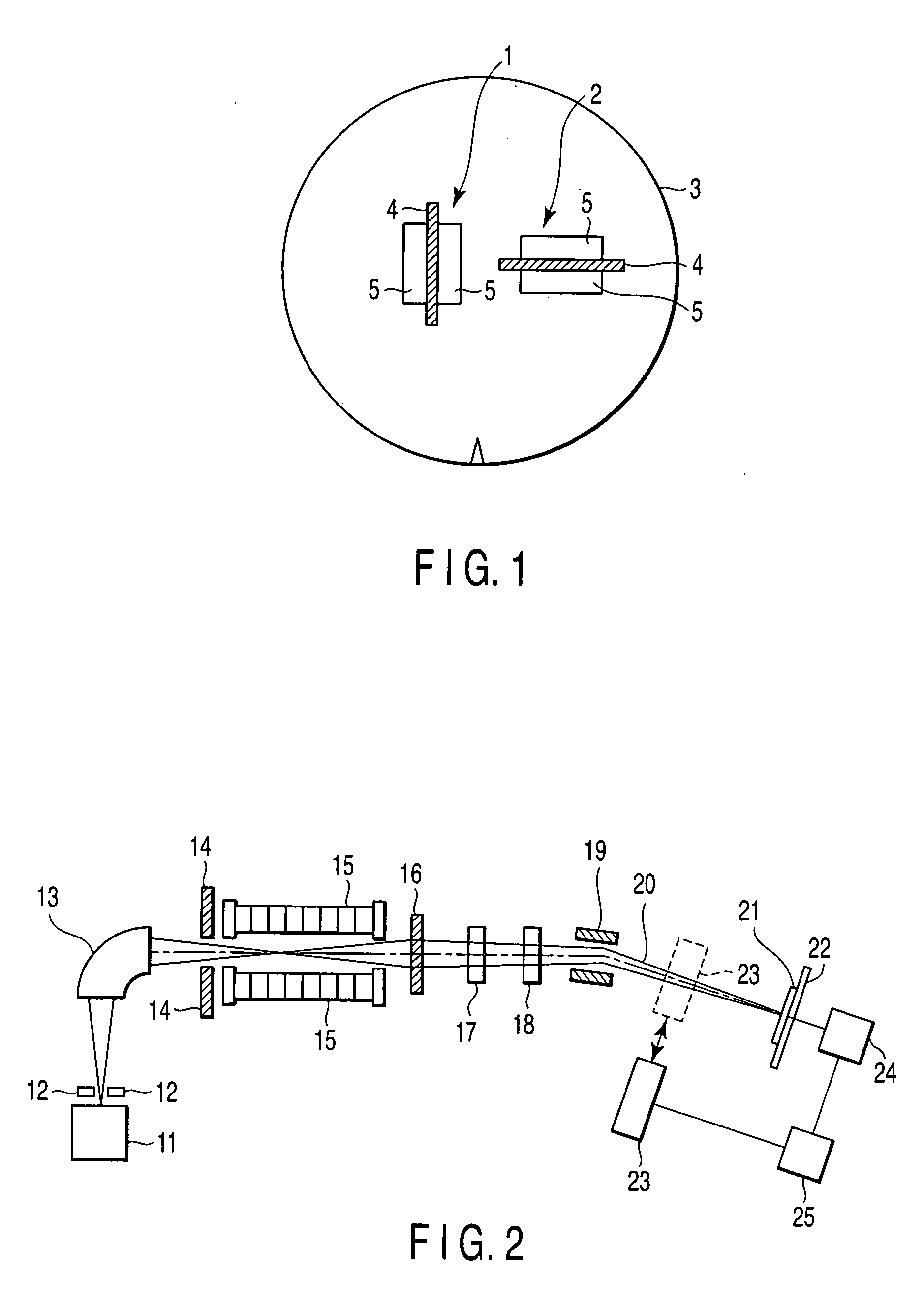
[0031]FIG. 1 is a diagram schematically showing a semiconductor wafer 3 on which a vertical MOS transistor 1 and a horizontal MOS transistor 2 are formed. Each of the vertical MOS transistor 1 and horizontal MOS transistor 2 comprises a gate electrode 4 and a source / drain diffusion layer 5. The vertical MOS transistor 1 and the horizontal MOS transistor 2 have a gate length (channel length) of not higher than 65 nm. The semiconductor wafer 3 is, for example, a Si wafer.

[0032] Studies by the present inventors indicate that a gate length (channel length) of not higher than 65 nm makes the asymmetry of the characteristics of the horizontal MOS transistor 2 more significant and that the asymmetry of the characteristics of the horizontal MOS transistor 2 cannot be sufficiently eliminated by adjusting the α and β angles.

[0033] The cause of the asymmetry of the transistor characteristics has been found to be a variation in the incident angle of ion beam, caused by eccentricity of the cen...

second embodiment

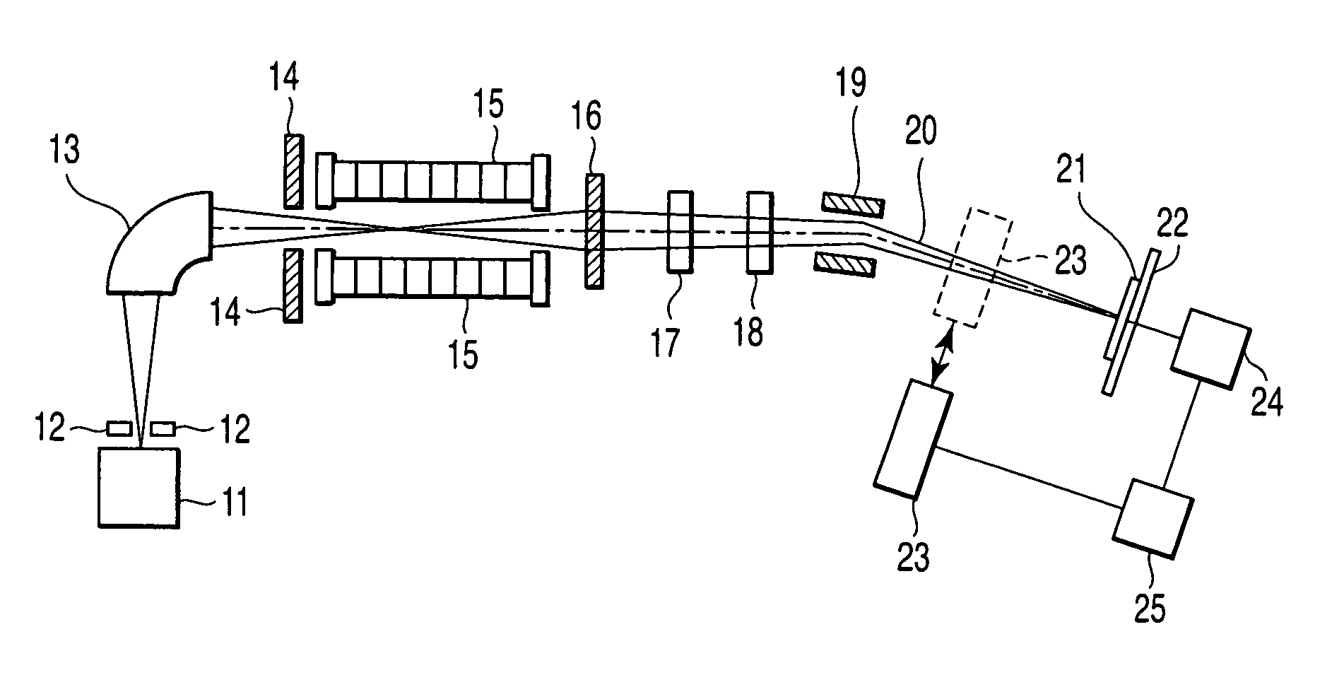
[0066]FIG. 16 is a diagram schematically showing an ion implanter according to the second embodiment of the present invention. FIG. 17 is a diagram schematically showing the configuration of an ion source chamber of the ion implanter according to the present embodiment. Parts of this ion implanter which correspond to those in FIG. 2 are denoted by the same reference numerals, with their detailed description omitted.

[0067] As previously described, eccentricity of the center of gravity of ion beam is considered to result from the spatial distribution of thermal electrons emitted from the cathode filament in the ion source chamber. Thus, in the present embodiment, the eccentricity of the center of gravity of the ion beam 20 is controlled by controlling the spatial distribution 37 of thermal electrons in the ion source chamber 11. The present embodiment will further be described below.

[0068] In FIG. 17, reference numeral 30 denotes a chamber. A gas introduction pipe 32 is provided in ...


PUM


Abstract

An ion implanter includes a sample stage for setting a sample having a main surface, an ion generating section configured to generate a plurality of ions, the ion generating section including a container into which an ion source gas is introduced and a filament for emitting thermal electrons provided in the container, an implanting section configured to implants an ion beam containing the plurality of ions in the main surface of the sample, and a control section configured to control a position of the sample or a spatial distribution of electrons emitted from the filament so that a direction of eccentricity of a center of gravity of the ion beam coincides with a direction of a normal line of the main surface.

Description

CROSS-REFERENCE TO RELATED APPLICATIONS [0001] This application is based upon and claims the benefit of priority from prior Japanese Patent Application No. 2004-193034, filed Jun. 30, 2004, the entire contents of which are incorporated herein by reference. BACKGROUND OF THE INVENTION [0002] 1. Field of the Invention [0003] The present invention relates to an ion implanter and a method of manufacturing a semiconductor device including an ion implanting process. [0004] 2. Description of the Related Art [0005] In recent years, large scale integrated circuits (LSI) have often been used in important parts of computers and communication apparatuses; the large scale integrated circuits are formed by connecting a large number of transistors and resistors together as electric circuits and integrating the circuits together on one chip. Thus, the performance of the whole apparatus depends strongly on the performance of a single LSI. The performance of the single LSI can be improved by increasi...

Claims


Application Information

Patent Timeline
Patent Type & Authority Applications(United States)
IPC IPC(8): H01J37/08
CPCH01J37/08H01J37/244H01J37/3171H01J2237/065H01J2237/31703H01J2237/20207H01J2237/2446H01J2237/24495H01J2237/24578H01J2237/083
Inventor ITOKAWA, HIROSHIKAWASE, YOSHIMASASUGURO, KYOICHI
Owner KK TOSHIBA
Why Eureka
Try Eureka