Display and displaying method

a display method and information technology, applied in non-linear optics, instruments, optics, etc., can solve the problems of low electric resistance required for these layers to be used as electrodes, and the transmission of 100% has not yet been achieved for transparent electrodes, etc., to achieve bright display, no dependence on viewing angles, and high light use efficiency

Inactive Publication Date: 2006-01-26
HITACHI LTD
View PDF10 Cites 22 Cited by
  • Summary
  • Abstract
  • Description
  • Claims
  • Application Information

AI Technical Summary

Benefits of technology

[0055] The display with the use of the electrochromic device is a non-light-emitting type display and is compared here with other non-light-emitting type displays. First, when compared with liquid crystal, the use of the electrochromic device of the present invention does not require a polarization plate, and therefore, efficiency of light use is high, and a bright display can be produced. In addition, there is a problem in liquid crystal that it has a narrow viewing angle or its brightness significantly differs depending on viewing angles. In the case of the electrochromic device, there is theoretically no dependency on viewing angles. Furthermore, rubbing of a substrate to orient liquid crystal molecules toward a specific direction is needed for liquid crystal, while there is no need of rubbing for the electrochromic device.
[0056] Furhter, in order to allow the substrate to be bent by the use of plastic as well as the display to be fabricated by a simple and low-cost printing process from now on, the electrochromic device is advantageous. Still further, fabrication in a wholly solid state is easier with the electrochromic device than with liquid crystal. The pixel size of a liquid crystal display is generally about 0.3 mm, and it is possible to form high-definition pixels with the electrochromic device that are equal to or of a higher definition than a liquid crystal display.
[0057] As for electronic paper, a microcapsule-type electrophoresis method is known. In this method, black (carbon black) and white (titanium dioxide) particles that are charged negatively and positively, respectively, are sealed into microcapsules, and color viewed from the obverse side is changed by allowing the particles to collect to the front side or the bottom side by means of applying an external electric field. The diameter of a particle is about 40 μm and the resolution of images depends upon the particle diameter. The advantages of the electrochromic device lie in that its cost is low because of no need for preparing special microcapsules, it can be more readily fabricated by coating or printing on electrodes compared with a display fabricated by the microcapsule electrophoresis method, and that the thickness of the whole device can be reduced because the thickness of the electrode layer can be made even thinner than 1 μm.
[0058] According to the above constitutions, the electrochromic device and the electrochromic display can be provided in a simple structure with high transmittance, which addresses the limitations of prior electrochromic and non-electrochromic display devices.

Problems solved by technology

At the same time, low electric resistance is required for these layers to be used as electrodes.
However, the transparent electrode is known to have absorption in the visible region, and the transmittance of 100% has not yet been achieved for the transparent electrode.

Method used


Image

  • Display and displaying method
  • Display and displaying method
  • Display and displaying method

Examples


first exemplary embodiment

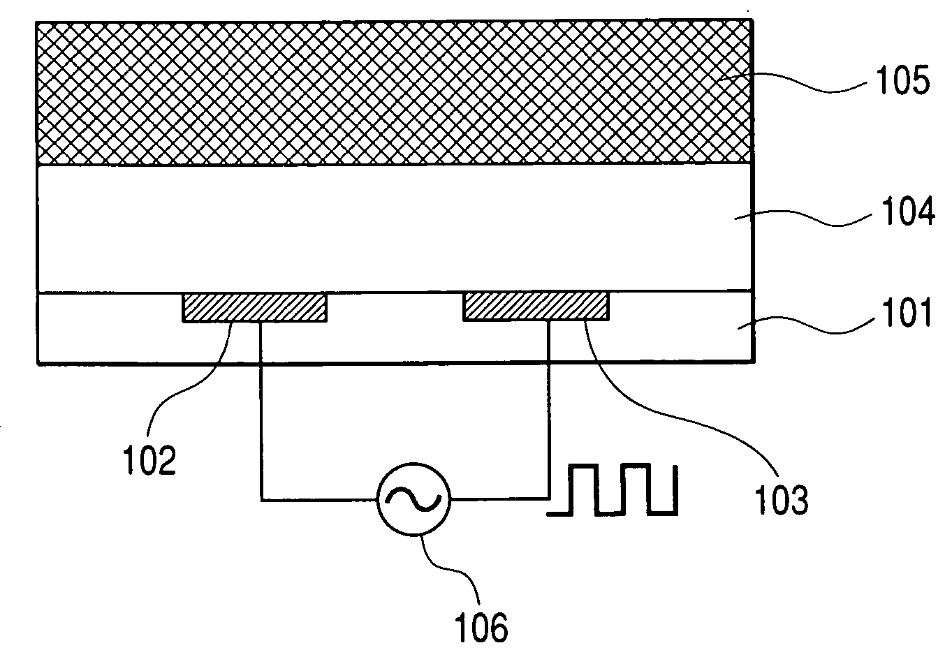
[0096] The Device and Operation

[0097] The fabrication method of an electrochromic device according to the present invention will now be explained. FIG. 14 illustrates the fabrication method of a device having the first structure using a first method. Part of a 3 cm square insulative glass substrate 361 with 1 mm thickness (FIG. 14A) is masked to form thereon two ITO electrodes 363 and 364 with a width of 5 mm and a thickness of 50 nm by magnetron sputtering (FIG. 14B). The electric resistance of the formed electrodes is 30 Ω / sq. Thereafter, an electrochromic layer 366 (FIG. 14C) with a thickness of 50 nm is formed on the substrate surface with the formed electrodes by spin coating a 5% by weight aqueous solution of a complex of poly(3,4-ethylenedioxythiophene)-polystyrenesulfonic acid for 60 sec at 4,300 rpm. A solution composed of 20% by weight of poly(ethylene oxide) with a molecular weight of 1×10⁶, 2% by weight of lithium perchlorate, and 78% by weight of tetrahydrofuran is app...

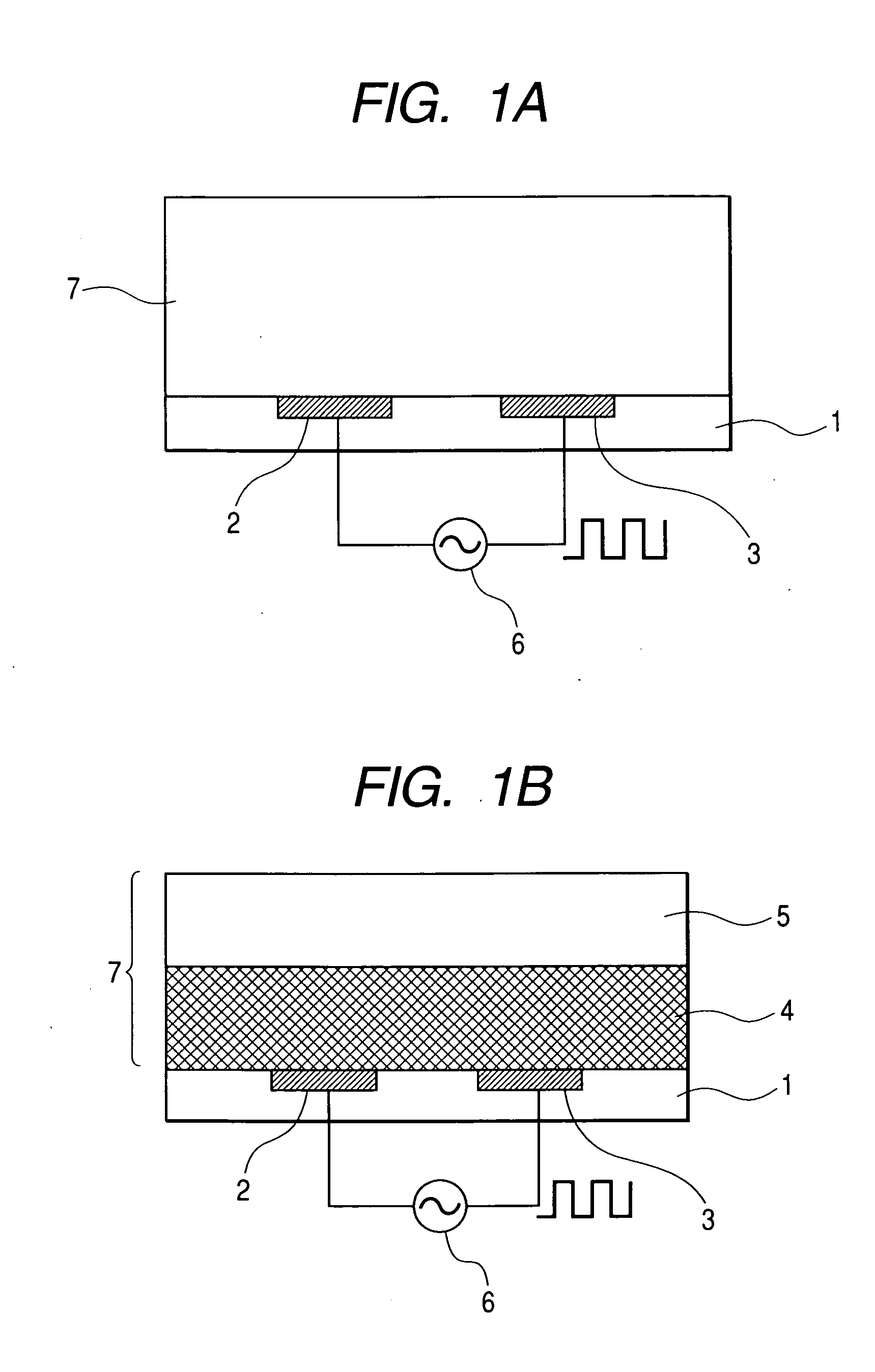
second exemplary embodiment

The Device and Operation

[0107] In the second embodiment, materials identical to those in the first embodiment were used. The fabrication of an electrochromic device having the second structure is explained. Part of a 3 cm square insulative glass substrate with 1 mm thickness was masked to form thereon two ITO electrodes with a width of 5 mm and a thickness of 50 nm by magnetron sputtering. The electric resistance of the formed electrodes was 30 Ω / sq. Then, an electrolyte layer with 1 μm thickness was formed on the substrate surface with the formed electrodes by spin coating a solution composed of 20% by weight of poly(ethylene oxide) with a molecular weight of 1×10⁶, 2% by weight of lithium perchlorate, and 78% by weight of tetrahydrofuran for 60 sec at 1,000 rpm. Subsequently, an electrochromic layer with 50 nm thickness was formed on the electrolyte layer by spin coating a 5% by weight aqueous solution of a complex of poly(3,4-ethylenedioxythiophene)-polystyrenesulfonic acid for...

third exemplary embodiment

[0113] An electrochromic device having the first structure of the present invention was fabricated in the same manner as that in the first embodiment except that tungsten oxide was used for the electrochromic compound and that n RF magnetron sputtering method was used to form the electrochromic layer. When a voltage was applied between the electrodes after connecting a power source to this device as in the first embodiment, reversible coloration resulted. Similarly when the device was fabricated using iridium oxide, nickel oxide, titanium dioxide, or vanadium oxide for the electrochromic compound, reversible coloration also resulted.


PUM

PropertyMeasurementUnit
transmittanceaaaaaaaaaa
thicknessaaaaaaaaaa

Abstract

An electrochromic device with high transmittance is for use as a display device. The electrochromic device includes at least a first and a second electrode formed on an insulative substrate and a conductive layer formed in contact with the insulative substrate, the first electrode, and the second electrode. Since an electrode layer functions in one layer, the transmittance through the device is enhanced, and the device can be fabricated in a simple process, allowing a reduction in the device fabrication costs.

Description

CLAIM OF PRIORITY [0001] The present application claims the benefit under 35 U.S.C. § 119 of the earlier filing date of Japanese Patent Application JP 2004-212460 which was filed on Jul. 21, 2004, the content of which is hereby incorporated by reference into the present application. BACKGROUND OF THE INVENTION [0002] 1. Field of the Invention [0003] The present invention relates to a display and a method for displaying information with the use of electrochromism. [0004] 2. Description of the Background [0005]“Electrochromism”, a phenomenon in which a compound color reversibly changes by applying a voltage, has been applied to electrochromic window glass and display devices. As shown below, conventionally known electrochromic devices have a structure in which an electrochromic layer and an electrolyte layer are sandwiched between a pair of electrodes, at least one of which being a transparent electrode, and electrochromism is generated by a voltage applied between these electrodes. T...

Claims


Application Information

Patent Timeline
Patent Type & Authority Applications(United States)
IPC IPC(8): G02F1/15
CPCG02F1/134363G02F2001/1557G02F1/155
Inventor KOJIMA, KYOKOTERAO, MOTOYASUMIYAMOTO, HARUKAZUHATANO, MUTSUKO
Owner HITACHI LTD
Why Eureka
Try Eureka