Snubber circuit
- Summary
- Abstract
- Description
- Claims
- Application Information
AI Technical Summary
Benefits of technology
Problems solved by technology
Method used
Image

Examples
first embodiment
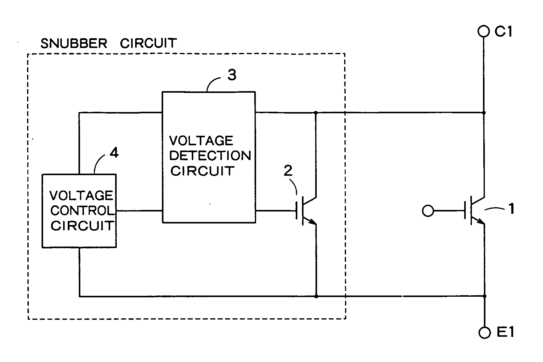
[0025]FIG. 1 is a block diagram showing a schematic structure of a snubber apparatus according to a First Embodiment of the present invention. The snubber apparatus in FIG. 1 is connected in parallel between a collector and an emitter of an IGBT 1 which is to be protected. As shown by a dotted line in the figure, the snubber circuit in FIG. 1 is provided with an IGBT 2 which is connected in parallel between the collector and emitter of the IGBT 1, a voltage detection circuit 3 which detects a voltage standing in correlation with the collector-emitter voltage of the IGBT 2 and a voltage control circuit 4 which controls a gate voltage of the IGBT 2 based on the detection result of the voltage detection circuit 3 and controls the collector-emitter voltage of the IGBT 1.
[0026] The voltage detection circuit 3 in FIG. 1 detects a collector-gate voltage of the IGBT 2 as a voltage standing in correlation with the collector-emitter voltage of the IGBT 1, but as will be described later, the ...
second embodiment
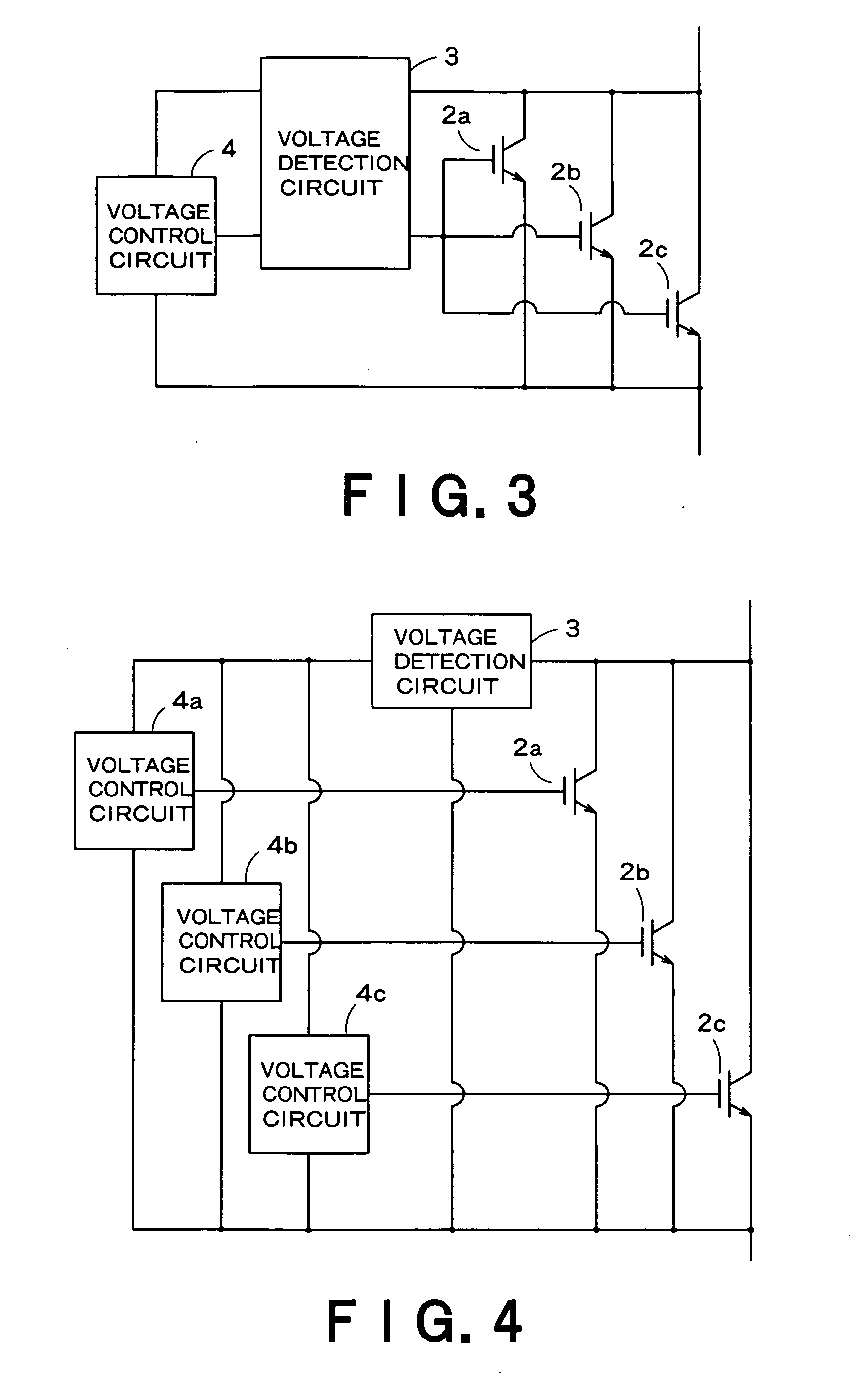
[0033] The IGBT to be protected is made up of a plurality of devices, and when the current capacity is large, the current capacity of the snubber circuit needs to be increased. In this case, the IGBT 2 is preferably made up of a plurality of devices.
[0034]FIG. 3 is a block diagram of a snubber circuit according to a Second Embodiment showing an example where a plurality of IGBTs 2 are connected in parallel. In FIG. 3, the IGBT 1 is omitted, but the IGBT 1 is connected in parallel to the IGBTs 2 as in the case of FIG. 1. The IGBT 1 will be omitted in all figures which will be explained hereafter, but suppose the IGBT 1 is actually connected in parallel to the IGBT 2 as in the case of FIG. 1.
[0035] The snubber circuit in FIG. 3 is provided with a plurality of IGBTs 2a, 2b and 2c connected in parallel between the collector and emitter of the IGBT 1 (not shown in FIG. 3), a voltage detection circuit 3 and a voltage control circuit 4. The voltage detection circuit 3 and the voltage con...
third embodiment
[0041] A Third Embodiment gives a concrete form to the inner structures of the voltage detection circuit 3 and the voltage control circuit 4 in the snubber circuit in FIG. 1.
[0042]FIG. 5 is a circuit diagram of a snubber circuit according to a Third Embodiment of the present invention. The basic structure of the snubber circuit in FIG. 5 is the same as that of the circuit in FIG. 1. The voltage detection circuit 3 is provided with a high breakdown voltage diode 5 and a capacitor 6 serially-connected between the collector and gate of the IGBT 2 and a differential amplifier 7 which outputs a voltage corresponding to a difference voltage between the voltage in a connection path between the high breakdown voltage diode 5 and the capacitor 6 and a predetermined reference voltage. The differential amplifier 7 need not always be a complicated circuit such as an operational amplifier and can be a source-grounded amplifier in which a reference voltage is connected to a source terminal of a ...
PUM
 Abstract
Description
Claims
Application Information
PatSnap Eureka turns technology decisions into work you can execute. Powered by our Innovation Knowledge Graph, it runs expert workflows across engineering, life sciences, materials and intellectual property. Get your review-ready output in minutes.


