Method for fabricating CMOS image sensor

a technology of image sensor and cmos, which is applied in the field of image sensor, can solve the problems of reducing yield, affecting the performance of the device protection layer, and contaminating the metal pad, so as to improve the device characteristics, prevent the contamination of the metal pad, and increase the yield

Inactive Publication Date: 2006-01-26
DONGBU ELECTRONICS CO LTD
View PDF16 Cites 5 Cited by
  • Summary
  • Abstract
  • Description
  • Claims
  • Application Information

AI Technical Summary

Benefits of technology

[0011] An object of the present invention is to provide a method for fabricating a CMOS image sensor, which improves device characteristics by preventing contamination of a metal pad without causing damage to a micro-lens.
[0012] Another object of the present invention is to provide a method for fabricating a CMOS image sensor, which enables formation of a reliable electrical contact when performing a wire bonding with respect to a metal pad.
[0013] Another object of the present invention is to provide a method for fabricating a CMOS image sensor, which increases yield.
[0015] Another object of the present invention is to provide a method for fabricating a CMOS image sensor, which enables a minimization of incidental damage to a material layer for micro-lens formation.

Problems solved by technology

According to a contemporary CMOS image sensor fabrication method, however, the color filter formation, planarization, and micro-lens formation processes generate a variety of residues that remain on the surface of the exposed metal pad, whereby the metal pad becomes contaminated and thus experiences corrosion due to the alkaline properties of the residue.
When a wire bonding process is subsequently performed with respect to the metal pad, such damage of the exposed metal pad is likely to result in an unreliable electrical contact, thereby lowering yield.
Although the color filter formation, planarization steps, and micro-lens formation may be performed while the device protection layer remains intact, if the metal pad opening were to be formed after micro-lens formation, the surface of the micro-lens is damaged during the etching of the device protection layer.
A damaged lens surface causes uncontrollable light diffusion in the micro-lens and can destroy its light-focusing properties, which severely degrades picture quality.

Method used


Image

  • Method for fabricating CMOS image sensor
  • Method for fabricating CMOS image sensor
  • Method for fabricating CMOS image sensor

Examples


Embodiment Construction

[0022] Reference will now be made in detail to the preferred embodiments of the present invention, examples of which are illustrated in the accompanying drawings. Wherever possible, like reference numbers will be used throughout the drawings to refer to the same or similar parts.

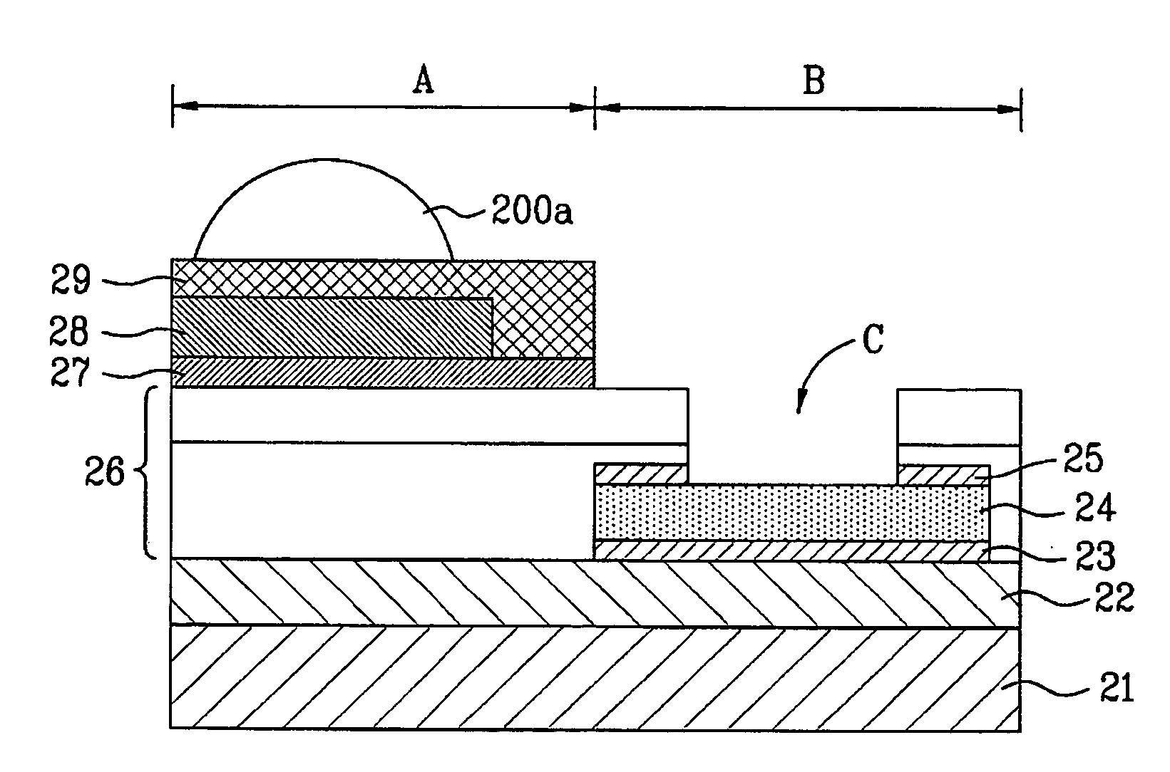
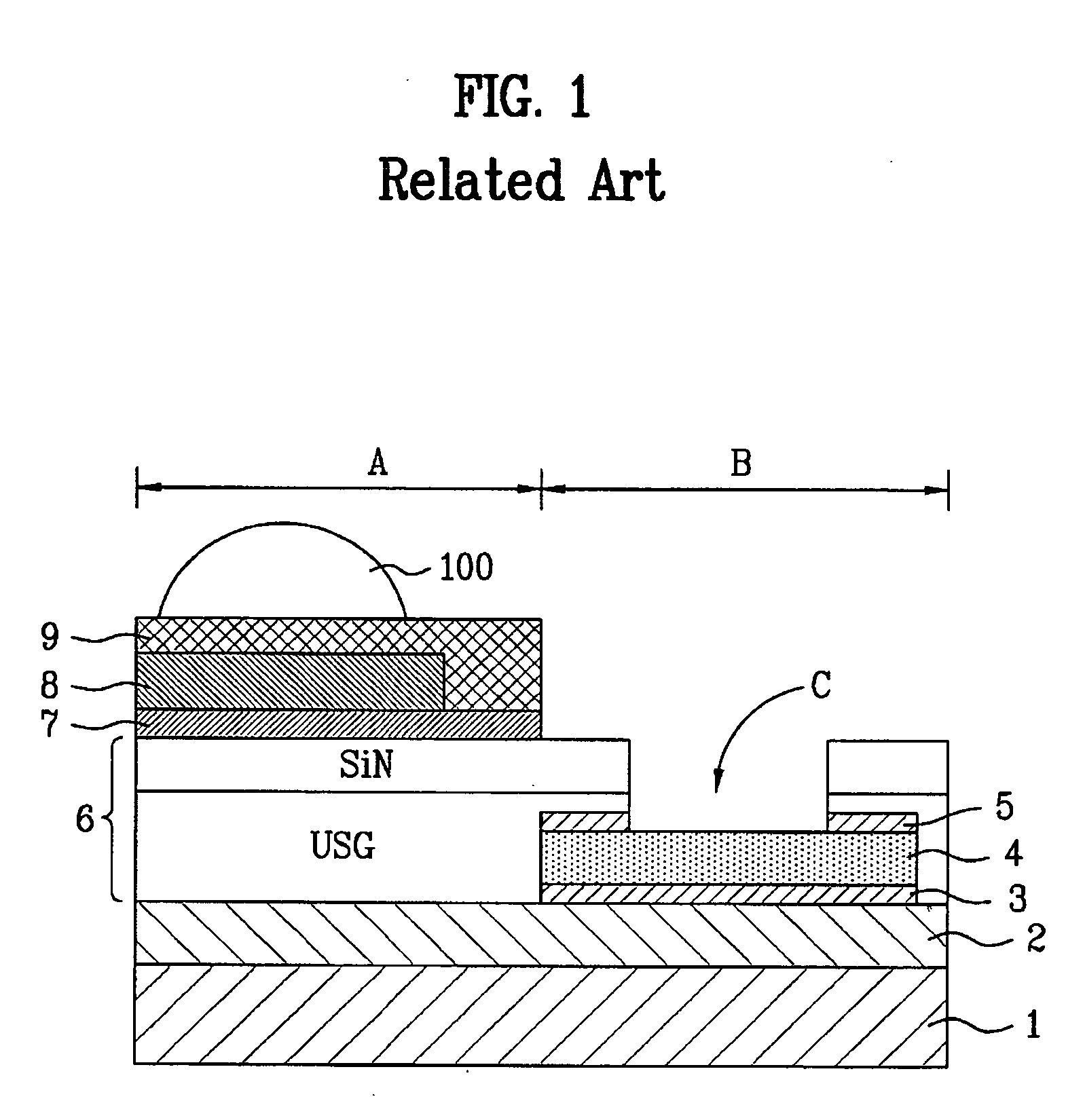
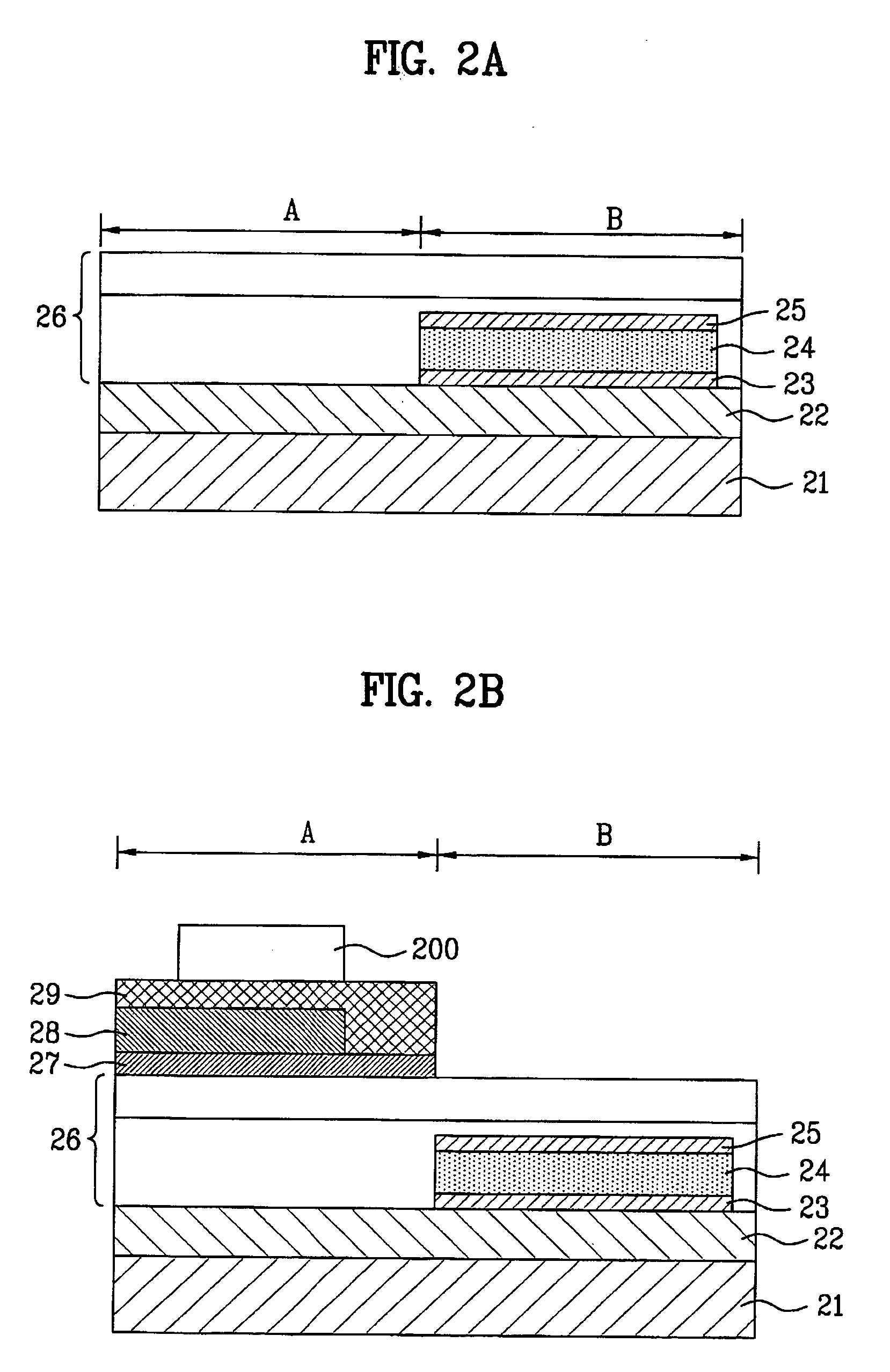
[0023] In the method for fabricating a CMOS image sensor according to the present invention, the step for forming an opening over a metal pad by a selective removal (etching) of a device protection layer covering the metal pad is performed after the step for depositing and patterning a material layer for formation of a micro-lens to be disposed over the photo-sensing device area. Yet, the reflow process is performed after the metal pad opening process, that is, in a state where the metal pad opening exists in the device protection layer. The CMOS image sensor fabrication method according to the present invention is illustrated in FIGS. 2A-2D, showing a photo-sensing device A and an adjacently disposed logic...


PUM


Abstract

A method for fabricating a CMOS image sensor improves the characteristics of device by preventing a pad from being contaminated without damaging a micro-lens. The method includes steps of forming a device protection layer on a semiconductor substrate including at least one photo-sensing device and at least one metal pad disposed in a logic circuit area corresponding to the at least one photo-sensing device, the device protection layer covering the at least one metal pad; forming each of a first planarization layer, a color filter layer, and a second planarization layer in sequence on the device protection layer in correspondence with the at least one photo-sensing device; forming on the second planarization layer a material layer for micro-lens formation; exposing a predetermined portion of the metal pad by selectively etching the device protection layer; and forming a micro-lens for directing incident light onto the at least one photo-sensing device by reflowing, after the exposing step, the material layer for micro-lens formation.

Description

CROSS-REFERENCE TO RELATED APPLICATIONS [0001] This application claims the benefit of Korean Application No. 10-2004-0056370 filed on Jul. 20, 2004, which is hereby incorporated by reference as if fully set forth herein. BACKGROUND OF THE INVENTION [0002] 1. Field of the Invention [0003] The present invention relates to an image sensor, and more particularly, to a method for fabricating a CMOS image sensor, which improves device characteristics by preventing contamination of a metal pad without causing damage to a micro-lens. [0004] 2. Discussion of the Related Art [0005] A complementary metal-oxide-semiconductor (CMOS) image sensor, which may be comprised of an array of photodiodes as the photo-sensing means and includes a CMOS logic circuit for each photodiode, is essentially a semiconductor device for generating an optical image based on incident light signals. In such a CMOS image sensor, wherein each photodiode senses incident light and the corresponding CMOS logic circuit conv...

Claims


Application Information

Patent Timeline
Patent Type & Authority Applications(United States)
IPC IPC(8): H01L21/00
CPCH01L27/14685H01L27/14627H01L27/146H01L31/10
Inventor SU KON, KIM
Owner DONGBU ELECTRONICS CO LTD
Why Eureka
Try Eureka