Novel film for copper diffusion barrier

a diffusion barrier and copper technology, applied in the direction of semiconductor devices, semiconductor/solid-state device details, electrical apparatus, etc., can solve the problems of increasing problems, limited speed at which future circuits will operate, and unstable in the presence of atmospheric moistur

Inactive Publication Date: 2006-01-26
NOVELLUS SYSTEMS
View PDF18 Cites 277 Cited by
  • Summary
  • Abstract
  • Description
  • Claims
  • Application Information

AI Technical Summary

Problems solved by technology
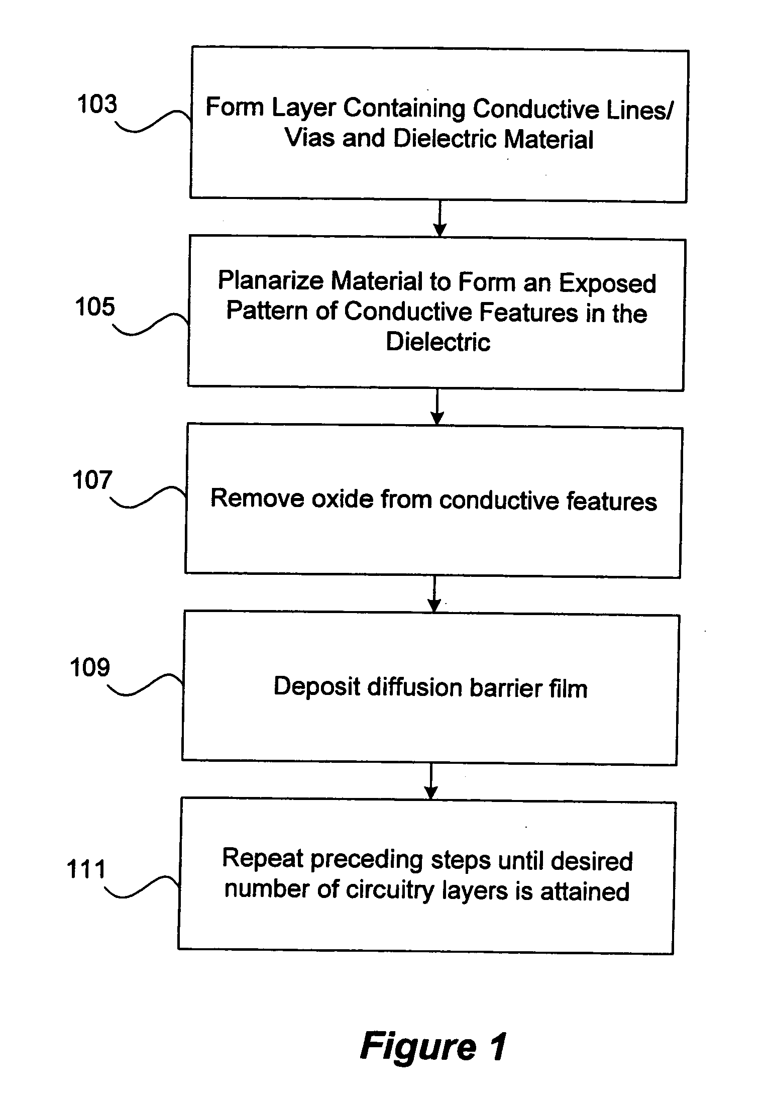
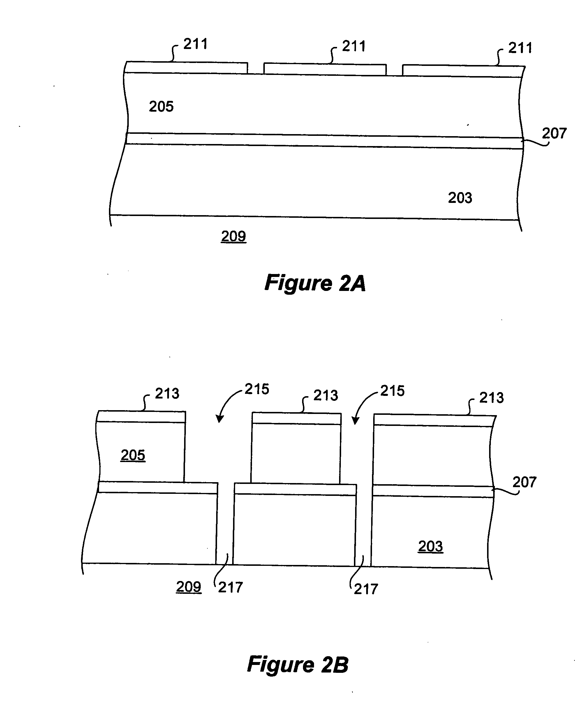
Without improvement in the insulator material, there will be increased problems due to capacitive effects such as coupling (crosstalk) and propagation delay.
The speed at which future circuits will operate will be limited by RC delay in the interconnect.
Although boron-doped silicon nitride has a lower dielectric constant than pure silicon nitride, it has proven to be unstable in the presence of atmospheric moisture.
Over time, the dielectric constant of boron-doped silicon nitride tends to increase, rapidly becoming unsuitable for use as a low dielectric constant copper diffusion barrier.

Method used


Image

  • Novel film for copper diffusion barrier
  • Novel film for copper diffusion barrier
  • Novel film for copper diffusion barrier

Examples


Embodiment Construction

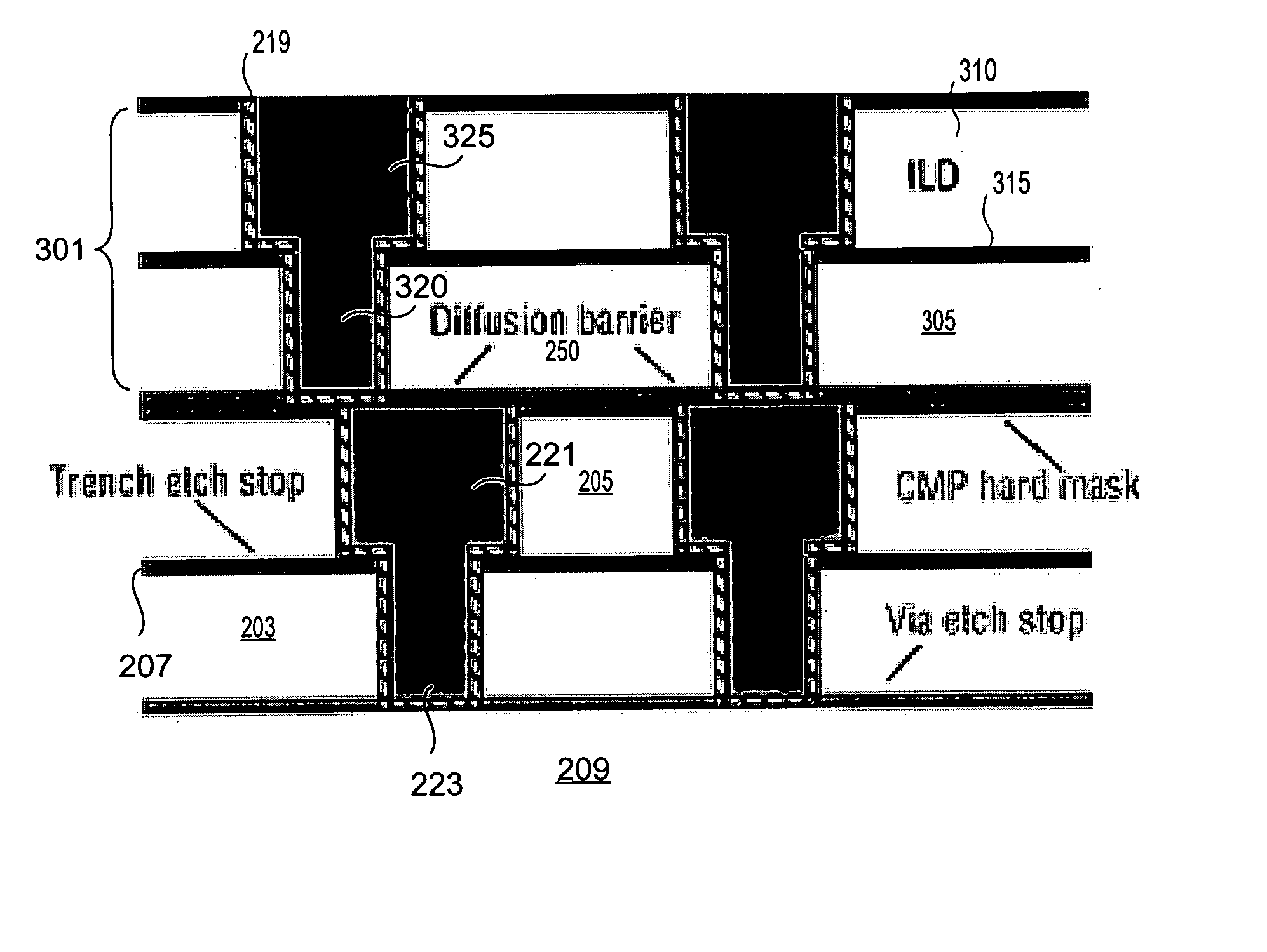
[0022] Boron nitride films having a dielectric constant of approximately 2.7 have been prepared by atmospheric chemical vapor deposition (“CVD”) at a high temperature. However, if exposed to air, these boron nitride films absorb moisture from the air and their dielectric constant increases substantially. Although boron-doped silicon nitride has a lower dielectric constant than pure silicon nitride, it has also proven to be unstable in the presence of atmospheric moisture. Over time, the dielectric constant of boron-doped silicon nitride tends to increase, rapidly becoming unsuitable for use as a copper diffusion barrier for the next generation of semiconductor device.

[0023] The term “semiconductor device” as used herein refers to any device formed on a semiconductor substrate or any device possessing a semiconductor material. In many cases, a semiconductor device participates in electronic logic or memory, or in energy conversion. The term “semiconductor device” subsumes partially ...


PUM

PropertyMeasurementUnit
temperaturesaaaaaaaaaa
pressuresaaaaaaaaaa
frequenciesaaaaaaaaaa

Abstract

The present invention provides a low dielectric constant copper diffusion barrier film suitable for use in a semiconductor device and methods for fabricating such a film. Some embodiments of the film are formed of a silicon-based material doped with boron. Other embodiments are formed, at least in part, of boron nitride. Some such embodiments include a moisture barrier film that includes oxygen and / or carbon. Preferred embodiments of the copper diffusion barrier maintain a stable dielectric constant of less than 4.5 in the presence of atmospheric moisture.

Description

BACKGROUND [0001] This invention relates to low dielectric constant layers for use in various applications. The invention also relates to methods of forming low dielectric constant layers in a wide range of VLSI fabrication operations. [0002] As the features of microelectronic integrated circuits devices are reduced to smaller sizes, the electrical properties of the materials that constitute the devices will require change and improvement. One material that must be improved is the electrical insulator (“dielectric”) used between the wires, metal lines, and other elements of the circuit. Without improvement in the insulator material, there will be increased problems due to capacitive effects such as coupling (crosstalk) and propagation delay. The speed at which future circuits will operate will be limited by RC delay in the interconnect. [0003] These difficulties can be mitigated by preparing the circuit using an inter-layer dielectric (“ILD”) having a dielectric constant that is as ...

Claims


Application Information

Patent Timeline
Patent Type & Authority Applications(United States)
IPC IPC(8): H01L21/4763H01L21/31H01L21/768H01L23/48
CPCH01L21/76807H01L21/76829H01L23/53295H01L2924/0002H01L2924/00
Inventor YU, YONGSIKBILLINGTON, KARENHEPBURN, ROBERTCARRIS, MICHAELCREW, WILLIAM
Owner NOVELLUS SYSTEMS
Why Eureka
Try Eureka