Field-effect transistor

a field-effect transistor and transistor technology, applied in the field of field-effect transistors, can solve the problems of loss, isolation, degradation of various high-frequency characteristics, etc., and achieve the effects of reducing side gate effect, preventing the miniaturization of transistors, and reducing transistor characteristics

Inactive Publication Date: 2006-02-02
COLLABO INNOVATIONS INC
View PDF3 Cites 35 Cited by
  • Summary
  • Abstract
  • Description
  • Claims
  • Application Information

AI Technical Summary

Benefits of technology

[0015] According to the conventional GaAs FET, since the finger portions 123a and 124a of the source electrode 123 and the drain electrode 124 are formed on the GaAs layer 135 of the mesa 121, a metallic-metallic bond is formed between the finger portions 123a and 124a, and the semiconductor layer, so that an ohmic junction is formed. Since the common portions 123b and 124b of the source electrode 123 and the drain electrode 124 are formed on the substrate 131, a metallic-semiconductor junction is formed between the common portions 123b and 124b, and the semiconductor layer, so that a Schottky junction is formed. With the Schottky junction formed between the source electrode 123 and the semiconductor layer, in the case where a potential difference is generated between the drain and the source, the electrons move from the source side to the drain side. As a result, a leakage current flows (i.e. side gate effect). The conventional GaAs FET, therefore, degrades field-effect transistor characteristics. More precisely, the electrons that have moved to the drain side prevent a depletion layer from being enlarged, which causes degradation of various high-frequency characteristics such as insertion loss, isolation and the like. In order to reduce such side gate effect, it is necessary to maintain a certain distance between drain and source. This prevents the miniaturization of the transistor.
[0016] The present invention is conceived in view of the above problem, and an object of the present invention is to provide a small field-effect transistor that can reduce degradation of the field-effect transistor characteristics.

Problems solved by technology

More precisely, the electrons that have moved to the drain side prevent a depletion layer from being enlarged, which causes degradation of various high-frequency characteristics such as insertion loss, isolation and the like.

Method used


Image

  • Field-effect transistor
  • Field-effect transistor
  • Field-effect transistor

Examples


first embodiment

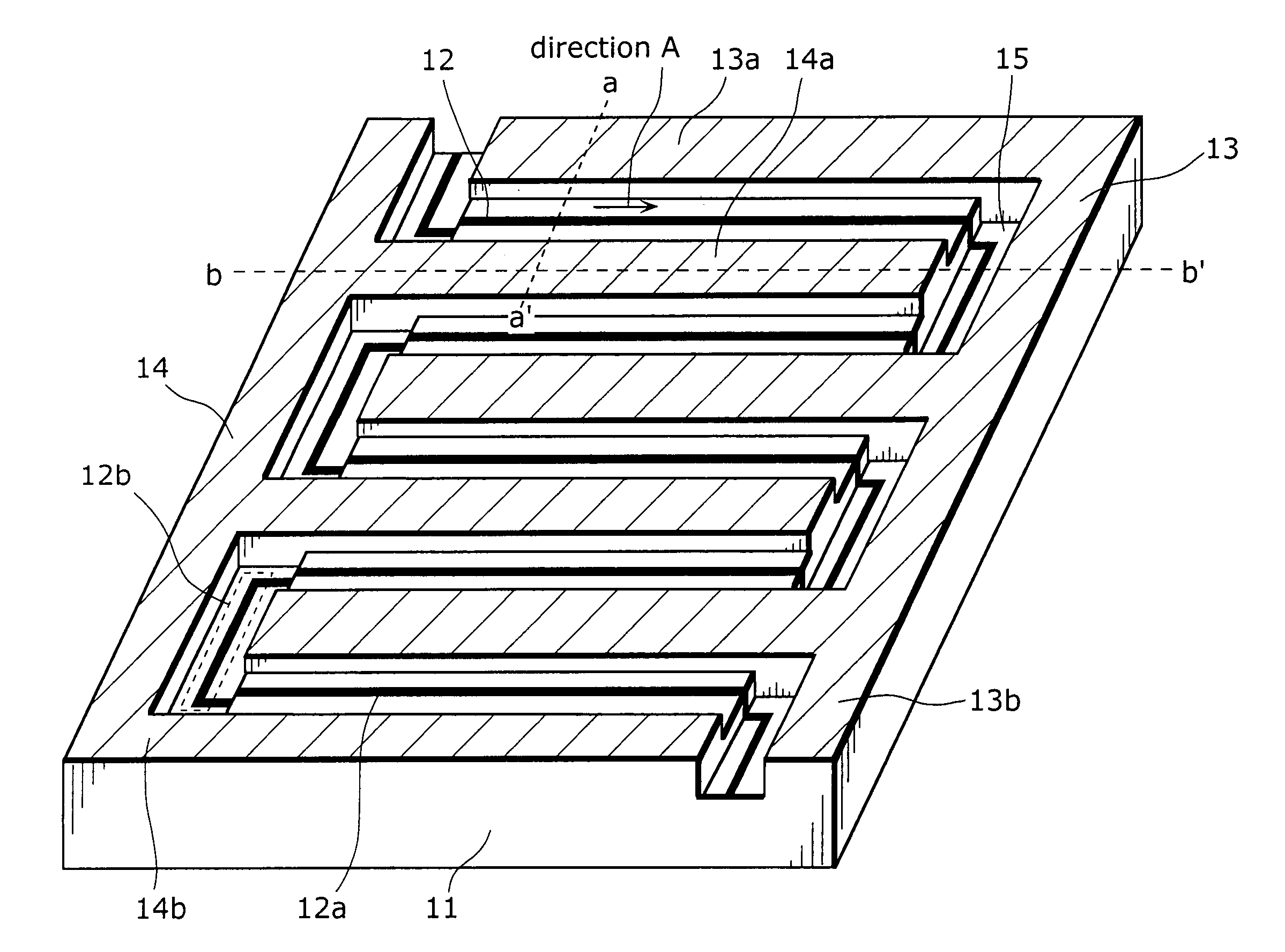
[0046]FIG. 4A shows an outer view of the GaAs FET according to the present embodiment and FIG. 4B shows a top view of the GaAs FET, while FIG. 4C shows a cross-sectional view of the GaAs FET, at the line b-b′ shown in FIG. 4A, and FIG. 4D shows a cross-sectional view of the GaAs FET at the line a-a′ shown in FIG. 4A.

[0047] The GaAs FET is comprised of a substrate 31 made of semi-insulating GaAs, and an epitaxial layer 30 formed by mesa separation due to an element separation region after a semiconductor layer is grown by crystal growth on the substrate 31. The epitaxial layer 30 includes the following layers which are sequentially stacked: a buffer layer 332 which has a thickness of 1 μm and is made of undoped GaAs, for alleviating lattice mismatch between the epitaxial layer 30 and the substrate 31,; a buffer layer 33 made of undoped AlGaAs; a channel layer 34 which is made of undoped In0.2Ga0.8As with a thickness of 20 nm, and in which carriers run; a spacer layer 35 made of undo...

second embodiment

[0060]FIG. 6A shows an outer view of the GaAs FET of the present embodiment and FIG. 6B shows a top view of the GaAs FET, while FIG. 6C shows a cross-sectional view of the GaAs FET at the line b-b′ shown in FIG. 6A and FIG. 6D shows a cross-sectional view of the GaAs FET at the line a-a′ shown in FIG. 6A.

[0061] The GaAs FET is comprised of a substrate 31 and an epitaxial layer 30. The epitaxial layer 30 is structured by sequentially stacking the buffer layers 32 and 33, the channel layer 34, the spacer layer 35, the carrier supplying layer 36, the Schottky layer 37 and the contact layer 38. Here, the source electrode 13 and the drain electrode 14 are formed on the contact layer 38. In the area between the source electrode 13 and the drain electrode 14, etching is performed on the contact layer 38 so that the surface of the Schottky layer 37 is exposed as a surface of the epitaxial layer 30, and the gate electrode 12 is formed on the Schottky layer 37 thus exposed.

[0062] The GaAs F...


PUM


Abstract

The present invention, which aims to provide a gallium arsenide field-effect transistor that can reduce degradation of field-effect transistor characteristics, and to realize miniaturization of the transistor, includes: a substrate; a mesa which includes a channel layer and is formed on the substrate; a source electrode formed on the mesa; a drain electrode; and a gate electrode, wherein, on the mesa, a top pattern is formed in which finger portions of the source electrode and the drain electrode which are formed in comb-shape are located so as to interdigitate, and a gate electrode is formed between the source electrode and the drain electrode, while common portions, which are base parts of the finger portions of the source and drain electrodes, are formed on the surface of the mesa, and the part located below the straight portion which is parallel to the finger portions of the gate electrode is electrically separated from the part located below a corner portion that connects neighboring straight portions of the gate electrode.

Description

BACKGROUND OF THE INVENTION [0001] (1) Field of the Invention [0002] The present invention relates to a field-effect transistor, and in particular, to a process of manufacturing the field-effect transistor that operates with stability, which allows the transistor to be miniaturized. [0003] (2) Description of the Related Art [0004] As a field-effect transistor (hereinafter to be referred to as “FET”), a gallium arsenide field-effect transistor (hereinafter to be referred to as “GaAs FET”) as disclosed in Japanese Laid-Open Patent Application No. 6-163604 can be taken as an example. FIG. 1 is a cross-sectional view of a structure of the GaAs FET described in the patent literature as mentioned above. [0005] In the GaAs FET, a mesa 141 having a channel layer (i.e. active layer) is formed on a semi-insulating substrate 140, while a gate electrode 142, a source electrode 143 and a drain electrode 144 are formed on the mesa 141. [0006]FIG. 2 is a top view of the GaAs FET having the structu...

Claims


Application Information

Patent Timeline
Patent Type & Authority Applications(United States)
IPC IPC(8): H01L31/0328
CPCH01L29/045H01L29/812H01L29/66856
Inventor MASUMOTO, YASUYUKIWATANABE, ATSUSHIHIDAKA, KENICHIYASUDA, EIJI
Owner COLLABO INNOVATIONS INC
Why Eureka
Try Eureka